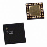
TZA3047BVH/C1,551 NXP Semiconductors, TZA3047BVH/C1,551 Datasheet - Page 7

TZA3047BVH/C1,551
Manufacturer Part Number
TZA3047BVH/C1,551
Description
IC LASER DRIVER 1.25GBPS 32-HBCC
Manufacturer
NXP Semiconductors
Type
Laser Diode Driver (Fiber Optic)r
Datasheet
1.TZA3047BVHC1551.pdf
(28 pages)
Specifications of TZA3047BVH/C1,551
Data Rate
1.25Gbps
Number Of Channels
1
Voltage - Supply
3.14 V ~ 3.47 V
Current - Supply
40mA
Current - Modulation
100mA
Current - Bias
100mA
Operating Temperature
-40°C ~ 85°C
Package / Case
32-HBCC
Mounting Type
Surface Mount
Lead Free Status / RoHS Status
Lead free / RoHS Compliant
Other names
568-1189
935270561551
TZA3047BVHW-S
935270561551
TZA3047BVHW-S
Philips Semiconductors
7
7.1
The TZA3047 operates with differential Positive Emitter
Coupled Logic (PECL), Low Voltage Positive Emitter
Coupled Logic (LVPECL) and Current-Mode Logic (CML)
data and clock inputs with a voltage swing from 100 mV to
1 V (p-p). It is assumed that both the data and clock inputs
carry a complementary signal with the specified
peak-to-peak value (true differential excitation).
The circuit generates an internal common mode voltage
for AC-coupled data and clock inputs and for single-ended
applications.
If V
pins and corresponds to an optical ‘one’ level of the laser.
7.2
The retiming function synchronizes the data with the clock
to improve the jitter performance. The data latch switches
on the rising edge of the clock input. The retiming function
is disabled when both clock inputs are below 0.3 V.
At start-up the initial polarity of the laser is unknown before
the first rising edge of the clock input.
2003 Jun 05
handbook, full pagewidth
30 Mbits/s up to 1.25 Gbits/s laser drivers
DIN
FUNCTIONAL DESCRIPTION
> V
Data and clock input
Retiming
DINQ
, the modulation current is sunk by the LA
V CCA
V CCD
TEST
DINQ
CINQ
GND
DIN
CIN
1
2
3
4
5
6
7
8
9
10
32
Fig.2 Pin configuration.
11
31
30
TZA3047A
TZA3047B
12
13
29
7
7.3
The on-duration of the laser current can be adjusted from
R
PWA is 100 pF. Pulse width adjustment is disabled when
pin PWA is short-circuited to ground.
7.4
The output stage is a high-speed bipolar differential pair
with typical rise and fall times of 120 ps and with a
modulation current source of up to 100 mA when the LA
pins are connected to V
The modulation current switches between the LA and LAQ
outputs. For a good RF performance the inactive branch
carries a small amount of the modulation current.
The LA output is optimized for the laser allowing a 2 V
dynamic range and a 1.2 V minimum voltage. The LAQ
output is optimized for the dummy load.
The output stage of the TZA3047A is optimized for
AC-coupled lasers and the output stage of the TZA3047B
is optimized for DC-coupled lasers.
The BIAS output is optimized for low voltage requirements
(0.4 V minimum for a 3.3 V laser supply; 0.8 V minimum
for a 5 V laser supply).
28
14
100 to +100 ps. The adjustment time is set by resistor
PWA
15
27
. The maximum allowable capacitive load on pin
Pulse width adjustment
Modulator output stage
16
26
19
18
17
25
24
23
22
21
20
MDB318
BIAS
GND
LA
LA
LAQ
LAQ
GND
PWA
TZA3047A; TZA3047B
CCO
.
Product specification


