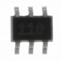
ZXLD1100H6TA Diodes Zetex, ZXLD1100H6TA Datasheet - Page 3

ZXLD1100H6TA
Manufacturer Part Number
ZXLD1100H6TA
Description
IC LED DRVR WHITE BCKLGT SC-70-6
Manufacturer
Diodes Zetex
Type
Backlight, White LEDr
Datasheet
1.ZXLD1100H6TA.pdf
(16 pages)
Specifications of ZXLD1100H6TA
Topology
PWM, Step-Up (Boost)
Number Of Outputs
1
Internal Driver
Yes
Type - Primary
Backlight
Type - Secondary
White LED
Frequency
1MHz
Voltage - Supply
2.5 V ~ 5.5 V
Voltage - Output
28V
Mounting Type
Surface Mount
Package / Case
SC-70-6, SC-88, SOT-363
Operating Temperature
-40°C ~ 85°C
Current - Output / Channel
50mA
Internal Switch(s)
Yes
Efficiency
80%
Lead Free Status / RoHS Status
Lead free / RoHS Compliant
Other names
UZXLD1100H6TA
UZXLD1100H6TR
UZXLD1100H6TR
ZXLD1100H6TR
UZXLD1100H6TR
UZXLD1100H6TR
ZXLD1100H6TR
Available stocks
Company
Part Number
Manufacturer
Quantity
Price
Part Number:
ZXLD1100H6TA
Manufacturer:
ZETEX
Quantity:
20 000
ISSUE 4 - JULY 2004
ELECTRICAL CHARACTERISTICS (at V
NOTES:
(1) Production testing of the device is performed at 25°C. Functional operation of the device over a -40°C to +85°C temperature range is
(2) Nominal 'on' time (T
(3) When using the open circuit protection feature, the maximum output voltage under normal operation should be maintained below the
(4) This is the time for which the device remains active after the EN pin has been asserted low. This delay is necessary to allow the output to be
(5) The minimum PWM signal frequency during this mode of operation is to ensure that the device remains active during PWM control. This
(6) The maximum PWM signal frequency during this mode of operation should be kept as low as possible to minimize errors due to the turn-off
SYMBOL
V
I
V
I
f
T
T
I
R
I
V
V
V
V
I
I
T
∆T/T
f
A
IN
FB
LXpk
LX(leak)
ENL
ENH
LX
LPF
OFF
ON
EN(hold)
IN
FB
LX
OUT
OUT(MAX)
ENH
ENL
guaranteed by design, characterization and process control.
T
minimum value specified, in order to prevent possible disturbance of the current control loop.
maintained during dc PWM mode operation.
provides a continuous dc output current. For lower frequencies, the device will be gated 'on' and 'off' during PWM control.
delay of the device (see Enable pin turn-off delay).
LPF
ONnom
= {I
LX(pkdc
PARAMETER
Input voltage
Supply current
FB pin control voltage
FB pin input current
Operating frequency
LX output 'OFF' time
LX output 'ON' time
Switch peak current limit
Switch 'On' resistance
Switch leakage current
Controller output voltage
Controller output voltage with output
open circuit
EN pin High level Input voltage
EN pin Low level Input voltage
EN pin Low level input current
EN pin High level input current
EN pin turn off delay
PWM duty cycle range at ‘EN’ input for
filtered PWM control
Internal PWM low pass filter cut-off
frequency
Filter attenuation
) x L/V
ONnom
Quiescent
Shutdown
IN
} +200ns.
) is defined by the input voltage (V
(3)
(2)
(5)
(4)
IN
= 3V, T
IN
), coil inductance (L) and peak current (I
3
amb
CONDITIONS
V
Output not switching
V
L=10 H, V
I
L=10 H, V
I
V
Normal operation
VSENSE pin
open-circuit or
grounded
VSENSE connected to
Vout
Device active
Device in shutdown
V
V
V
high to low
10kHz < f < 100kHz,
V
f=30kHz
OUT
OUT
EN
EN
LX
EN
EN
EN
ENH
=20V
= V
= 0V
=20mA
=20mA
=0V
=V
switched from
= 25°C unless otherwise stated
=V
IN
IN
IN
, I
OUT
OUT
LX
= 0,
=10V,
=10V,
LXpkdc
MIN.
90.5
350
2.5
1.5
25
20
) according to the expression:
ZXLD1100
S E M I C O N D U C T O R S
TYP.
0.35
52.5
500
320
120
1.5
60
30
4
MAX. UNIT
109.5
(1)
-100
100
500
100
100
V
5.5
0.4
28
1
5
1
1
IN
)
MHz
mV
mA
kHz
nA
nA
µA
nA
dB
ns
µs
µs
%
V
V
V
V
V
A
A


