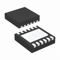
LT3498EDDB#TRMPBF Linear Technology, LT3498EDDB#TRMPBF Datasheet - Page 17

LT3498EDDB#TRMPBF
Manufacturer Part Number
LT3498EDDB#TRMPBF
Description
IC LED DRVR WT/OLED BCKLGT 12DFN
Manufacturer
Linear Technology
Type
Backlight, OLED, White LEDr
Datasheet
1.LT3498EDDBTRMPBF.pdf
(24 pages)
Specifications of LT3498EDDB#TRMPBF
Topology
PWM, Step-Up (Boost)
Number Of Outputs
1
Internal Driver
Yes
Type - Primary
Backlight
Type - Secondary
OLED, White LED
Frequency
1.8MHz ~ 2.8MHz
Voltage - Supply
2.5 V ~ 12 V
Voltage - Output
32V
Mounting Type
Surface Mount
Package / Case
12-DFN
Operating Temperature
-40°C ~ 85°C
Current - Output / Channel
20mA
Internal Switch(s)
Yes
No. Of Outputs
2
Output Current
200mA
Output Voltage
32V
Input Voltage
2.5V To 12V
Dimming Control Type
PWM / DC
Operating Temperature Range
-40°C To +85°C
Driver Case Style
DFN
Rohs Compliant
Yes
Lead Free Status / RoHS Status
Lead free / RoHS Compliant
Efficiency
-
Other names
LT3498EDDB#TRMPBFTR
Available stocks
Company
Part Number
Manufacturer
Quantity
Price
APPLICATIONS INFORMATION— LED AND OLED DRIVER
Board Layout Considerations
As with all switching regulators, careful attention must be
paid to the PCB board layout and component placement.
To prevent electromagnetic interference (EMI) problems,
proper layout of high frequency switching paths is essential.
Minimize the length and area of all traces connected to
the switching node pins (SW1 and SW2). Keep the sense
voltage pins (CAP1 and LED1) away from the switching
CTRL1
GND
CTRL2
V
OUT2
VIAS TO GROUND PLANE REQUIRED TO
IMPROVE THERMAL PERFORMANCE
VIAS TO V OUT2
R
FB2
FB2
LED1
Figure 13. Recommended Board Layout
1
2
3
4
5
6
R
SENSE1
GND
C3
C2
C1
node. The FB2 connection for the feedback resistor R
should be tied directly from the V
pin and be kept as short as possible, ensuring a clean,
noise-free connection. Place C
CAP1 and CAP2 pins respectively. Always use a ground
plane ender the switching regulator to minimize interplane
coupling. Recommended component placement is shown
in Figure 13.
12
11
10
9
8
7
V
OUT2
CAP1
CAP2
V
3498 F13
IN
L1
L2
SW1
SW2
C
IN
GND
OUT1
and C
OUT2
OUT2
pin to the FB2
LT3498
next to the
17
3498fa
FB2


