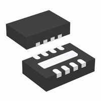
LTC3490EDD#PBF Linear Technology, LTC3490EDD#PBF Datasheet - Page 11

LTC3490EDD#PBF
Manufacturer Part Number
LTC3490EDD#PBF
Description
IC LED DRIVER PHOTO FLASH 8-DFN
Manufacturer
Linear Technology
Type
Photo Flash LEDr
Datasheet
1.LTC3490EDDPBF.pdf
(12 pages)
Specifications of LTC3490EDD#PBF
Constant Current
Yes
Topology
PWM, Step-Up (Boost)
Number Of Outputs
1
Internal Driver
Yes
Type - Primary
Flash/Torch
Type - Secondary
White LED
Frequency
1MHz ~ 1.6MHz
Voltage - Supply
1 V ~ 3.2 V
Voltage - Output
2.8 V ~ 4 V
Mounting Type
Surface Mount
Package / Case
8-DFN
Operating Temperature
-40°C ~ 85°C
Current - Output / Channel
350mA
Internal Switch(s)
Yes
Efficiency
90%
Led Driver Application
Lighting
No. Of Outputs
1
Output Current
350mA
Output Voltage
4V
Input Voltage
1V To 3.2V
Dimming Control Type
Analog
Rohs Compliant
Yes
Lead Free Status / RoHS Status
Lead free / RoHS Compliant
Available stocks
Company
Part Number
Manufacturer
Quantity
Price
PACKAGE DESCRIPTIO
3.5 ±0.05
2.15 ±0.05
RECOMMENDED SOLDER PAD PITCH AND DIMENSIONS
1.65 ±0.05
(2 SIDES)
0.25 ± 0.05
.030 ± .005
(0.203 – 0.254)
.008 – .010
TYP
NOTE:
1. DIMENSIONS IN
2. DRAWING NOT TO SCALE
3. THESE DIMENSIONS DO NOT INCLUDE MOLD FLASH OR PROTRUSIONS.
.245
MIN
2.38 ±0.05
(2 SIDES)
RECOMMENDED SOLDER PAD LAYOUT
MOLD FLASH OR PROTRUSIONS SHALL NOT EXCEED .006" (0.15mm)
(0.254 – 0.508)
0.50
BSC
Information furnished by Linear Technology Corporation is believed to be accurate and reliable.
However, no responsibility is assumed for its use. Linear Technology Corporation makes no represen-
tation that the interconnection of its circuits as described herein will not infringe on existing patent rights.
.010 – .020
.050 BSC
(0.406 – 1.270)
(MILLIMETERS)
.016 – .050
U
0.675 ±0.05
8-Lead Plastic Small Outline (Narrow .150 Inch)
INCHES
× 45°
PACKAGE
OUTLINE
8-Lead Plastic DFN (3mm × 3mm)
(Reference LTC DWG # 05-08-1610)
(Reference LTC DWG # 05-08-1698)
.045 ± .005
.160 ± .005
TOP MARK
(NOTE 6)
0°– 8° TYP
PIN 1
0.200 REF
S8 Package
DD Package
NOTE:
1. DRAWING TO BE MADE A JEDEC PACKAGE OUTLINE M0-229 VARIATION OF (WEED-1)
2. DRAWING NOT TO SCALE
3. ALL DIMENSIONS ARE IN MILLIMETERS
4. DIMENSIONS OF EXPOSED PAD ON BOTTOM OF PACKAGE DO NOT INCLUDE
5. EXPOSED PAD SHALL BE SOLDER PLATED
6. SHADED AREA IS ONLY A REFERENCE FOR PIN 1 LOCATION
MOLD FLASH. MOLD FLASH, IF PRESENT, SHALL NOT EXCEED 0.15mm ON ANY SIDE
ON TOP AND BOTTOM OF PACKAGE
(5.791 – 6.197)
.228 – .244
(1.346 – 1.752)
(0.355 – 0.483)
.053 – .069
.014 – .019
TYP
8
1
(4.801 – 5.004)
.189 – .197
0.75 ±0.05
3.00 ±0.10
2
(4 SIDES)
7
NOTE 3
6
3
0.00 – 0.05
5
4
1.65 ± 0.10
(2 SIDES)
(1.270)
.050
BSC
(3.810 – 3.988)
(0.101 – 0.254)
.150 – .157
.004 – .010
NOTE 3
BOTTOM VIEW—EXPOSED PAD
0.25 ± 0.05
SO8 0303
R = 0.115
TYP
4
5
2.38 ±0.10
(2 SIDES)
LTC3490
8
1
0.50 BSC
0.38 ± 0.10
11
(DD8) DFN 1203
3490fa


