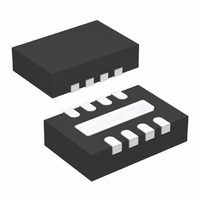
LTC3490EDD#PBF Linear Technology, LTC3490EDD#PBF Datasheet - Page 3

LTC3490EDD#PBF
Manufacturer Part Number
LTC3490EDD#PBF
Description
IC LED DRIVER PHOTO FLASH 8-DFN
Manufacturer
Linear Technology
Type
Photo Flash LEDr
Datasheet
1.LTC3490EDDPBF.pdf
(12 pages)
Specifications of LTC3490EDD#PBF
Constant Current
Yes
Topology
PWM, Step-Up (Boost)
Number Of Outputs
1
Internal Driver
Yes
Type - Primary
Flash/Torch
Type - Secondary
White LED
Frequency
1MHz ~ 1.6MHz
Voltage - Supply
1 V ~ 3.2 V
Voltage - Output
2.8 V ~ 4 V
Mounting Type
Surface Mount
Package / Case
8-DFN
Operating Temperature
-40°C ~ 85°C
Current - Output / Channel
350mA
Internal Switch(s)
Yes
Efficiency
90%
Led Driver Application
Lighting
No. Of Outputs
1
Output Current
350mA
Output Voltage
4V
Input Voltage
1V To 3.2V
Dimming Control Type
Analog
Rohs Compliant
Yes
Lead Free Status / RoHS Status
Lead free / RoHS Compliant
Available stocks
Company
Part Number
Manufacturer
Quantity
Price
SYMBOL
I
R
V
V
I
K
R
V
V
V
V
Note 1: Stresses beyond those listed under Absolute Maximum Ratings
may cause permanent damage to the device. Exposure to any Absolute
Maximum Rating condition for extended periods may affect device
reliability and lifetime.
Note 2: The LTC3490 is guaranteed to meet performance specifications
from 0°C to 70°C. Specifications over the –40°C to 85°C range are
assured by design, characterization and correlation with statistical process
controls.
Note 3: The LTC3490 input voltage may drop below the minimum start-up
voltage once the LED voltage has risen above 2.3V.
ELECTRICAL CHARACTERISTICS
temperature range, otherwise specifications are T
TYPICAL PERFOR A CE CHARACTERISTICS
L(PMOS)
IN
IH
IL
CTRL
IN(LOBAT1)
IN(LOBAT2)
IN(UVLO2)
IN(UVLO1)
ON(PMOS)
ON(LOBAT)
1.360
1.280
1.400
1.320
1.200
1.240
–50
Oscillator Frequency
vs Temperature
PARAMETER
Leakage Current, PMOS Switch
On-Resistance, PMOS Switch
Input High (CELLS)
Input High (SHDN)
Input Low (CELLS)
Input Low (SHDN)
Input Current (CTRL/SHDN, CELLS)
Control Gain, I
On-Resistance, LOBAT Output
Input Voltage, Low Battery, 1 Cell
Input Voltage, Low Battery, 2 Cells
Input Voltage, Undervoltage Lockout, V
2 Cells
Input Voltage, Undervoltage Lockout, V
1 Cell
TEMPERATURE (°C)
0
LED
/V
50
CTRL
W
3490 G01
U
100
CONDITIONS
Scales Linearity with V
V
V
V
IN
CELLS
CELLS
CELLS
CELLS
200
100
A
< V
400
350
300
250
150
50
= 25°C. V
0
IN(LOBAT)
= 0V
= V
= V
= 0 V
0
I
LED
IN
IN
vs V
The
0.2
IN
CTRL
●
= 2.5V unless otherwise specified.
MAXIMUM
denotes specifications which apply over the full operating
V
IN
0.4
CTRL
, V
Note 4: This device includes overtemperature protection intended to
protect the device during momentary overload conditions. The maximum
junction temperature may be exceeded when overtemperature protection
is active. Continuous operation above the specified maximum operating
junction temperature may result in device degradation or failure.
Note 5: The Exposed Pad of the DFN package must be soldered to a
PCB pad for optimum thermal conductivity. This pad must be connected
to ground.
/V
IN
IN
MINIMUM
= 1V
0.6
(V)
0.8
3490 G02
1
●
●
●
●
●
375
350
300
275
250
325
V
IN
1
I
MIN
0.8
1.8
1.4
0.7
LED
V
– 0.4
LED
vs V
= 3.5V
1.5
V
V
IN
IN
IN
0.13
0.01
TYP
500
0.1
• 0.9
• 0.2
V
IN
LTC3490
2
(V)
MAX
1.12
2.24
300
0.4
1.8
0.9
2.5
UNITS
mA/V
3490fa
3490 G03
3
µA
µA
Ω
Ω
V
V
V
V
V
V
V
V
3


