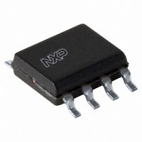
PCA9533D/01,112 NXP Semiconductors, PCA9533D/01,112 Datasheet - Page 5

PCA9533D/01,112
Manufacturer Part Number
PCA9533D/01,112
Description
IC LED DRIVER RGB 8-SOIC
Manufacturer
NXP Semiconductors
Type
RGB LED Driverr
Datasheet
1.PCA9533DP01118.pdf
(24 pages)
Specifications of PCA9533D/01,112
Package / Case
8-SOIC (3.9mm Width)
Topology
Open Drain, PWM
Number Of Outputs
4
Internal Driver
Yes
Type - Primary
Backlight, LED Blinker
Type - Secondary
RGB
Frequency
400kHz
Voltage - Supply
2.3 V ~ 5.5 V
Mounting Type
Surface Mount
Operating Temperature
-40°C ~ 85°C
Current - Output / Channel
25mA
Internal Switch(s)
Yes
Low Level Output Current
25 mA
Operating Supply Voltage
2.3 V to 5.5 V
Maximum Supply Current
550 uA
Maximum Power Dissipation
400 mW
Maximum Operating Temperature
+ 85 C
Mounting Style
SMD/SMT
Minimum Operating Temperature
- 40 C
Lead Free Status / RoHS Status
Lead free / RoHS Compliant
For Use With
568-4003 - DEMO BOARD LED DIMMER568-3512 - DEMO BOARD UART TO I2C
Voltage - Output
-
Efficiency
-
Lead Free Status / Rohs Status
Lead free / RoHS Compliant
Other names
568-3372-5
935274434112
PCA9533D/01
935274434112
PCA9533D/01
NXP Semiconductors
PCA9533_3
Product data sheet
6.2.1 Control register definition
6.3.1 INPUT - Input register
6.3.2 PCS0 - Frequency Prescaler 0
6.3.3 PWM0 - Pulse Width Modulation 0
6.3 Register descriptions
Table 4.
The INPUT register reflects the state of the device pins. Writes to this register will be
acknowledged but will have no effect.
Table 5.
Remark: The default value ‘X’ is determined by the externally applied logic level (normally
logic 1) when used for directly driving LED with pull-up to V
PSC0 is used to program the period of the PWM output.
The period of BLINK0 = (PSC0 + 1) / 152.
Table 6.
The PWM0 register determines the duty cycle of BLINK0. The outputs are LOW (LED on)
when the count is less than the value in PWM0 and HIGH (LED off) when it is greater. If
PWM0 is programmed with 00h, then the PWM0 output is always HIGH (LED off).
The duty cycle of BLINK0 = PWM0 / 256.
Table 7.
B2
0
0
0
0
1
1
Bit
Symbol
Default
Bit
Symbol
Default
Bit
Symbol
Default
B1
0
0
1
1
0
0
Register summary
INPUT - Input register description
PSC0 - Frequency Prescaler 0 register description
PSC0[7]
PWM0 - Pulse Width Modulation 0 register description
PWM0
[7]
B0
0
1
0
1
0
1
7
0
7
0
7
1
-
PSC0[6]
Symbol
INPUT
PSC0
PWM0
PSC1
PWM1
LS0
PWM0
Rev. 03 — 27 April 2009
[6]
6
0
6
0
6
0
-
PSC0[5]
PWM0
[5]
Access
read only
read/write
read/write
read/write
read/write
read/write
5
0
5
0
5
0
-
PSC0[4]
PWM0
[4]
4
0
4
0
4
0
-
Description
input register
frequency prescaler 0
PWM register 0
frequency prescaler 1
PWM register 1
LED selector
PSC0[3]
PWM0
LED3
[3]
X
3
3
0
3
0
DD
PSC0[2]
PWM0
.
LED2
4-bit I
[2]
2
X
2
2
0
0
2
C-bus LED dimmer
PCA9533
PSC0[1]
© NXP B.V. 2009. All rights reserved.
PWM0
LED1
[1]
X
1
1
0
1
0
PSC0[0]
PWM0
LED0
[0]
X
0
0
0
0
0
5 of 24


