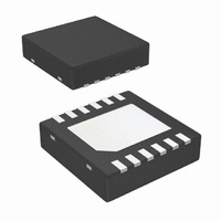
LM3553SD/NOPB National Semiconductor, LM3553SD/NOPB Datasheet - Page 8

LM3553SD/NOPB
Manufacturer Part Number
LM3553SD/NOPB
Description
IC LED DRIVER PHOTO FLASH 12-LLP
Manufacturer
National Semiconductor
Series
PowerWise®r
Type
Photo Flash LED (I²C Interface)r
Datasheet
1.LM3553SDNOPB.pdf
(18 pages)
Specifications of LM3553SD/NOPB
Topology
Step-Up (Boost)
Number Of Outputs
1
Internal Driver
Yes
Type - Primary
Backlight, Flash/Torch
Frequency
1MHz ~ 1.35MHz
Voltage - Supply
2.7 V ~ 5.5 V
Mounting Type
Surface Mount
Package / Case
12-LLP
Operating Temperature
-30°C ~ 85°C
Current - Output / Channel
1.2A
Internal Switch(s)
Yes
Efficiency
90%
Operating Supply Voltage (typ)
3.3/5V
Number Of Segments
2
Operating Temperature (min)
-30C
Operating Temperature (max)
85C
Operating Temperature Classification
Commercial
Package Type
LLP EP
Pin Count
12
Mounting
Surface Mount
Operating Supply Voltage (min)
2.7V
Operating Supply Voltage (max)
5.5V
For Use With
LM3553SDEV - BOARD EVALUATION FOR LM3553S
Lead Free Status / RoHS Status
Lead free / RoHS Compliant
Voltage - Output
-
Lead Free Status / Rohs Status
Compliant
Other names
LM3553SD
LM3553SD
LM3553SDTR
LM3553SD
LM3553SDTR
www.national.com
Block Diagram
Circuit Description
CIRCUIT COMPONENTS
F
The flash enable pin, F
I
'1', the flash current level defined through the I2C interface,
will be delived to the Flash LED. If the F
during the flash pulse, the flash event will stop. In the event
that F
will continue to deliver the flash current until the safety timer
duration (set through the I2C interface) is reached.
The LM3553 does not provide a fixed off-time after the flash
pulse has ended. Most flash LED manufacturers require that
the flash pulse duration be 10% of the total Flash cycle. Ex-
ample: If the flash pulse duration is set to be 200 milliseconds
(Flash Duration Code= 0011), the recommended off time for
the LED would be 1.8 seconds. Please consult the LED man-
ufacturers datasheet for exact timing requirements.
If the LM3553 is placed in indicator mode or torch mode
through the I
then low, at the end of the flash event, the LM3553 will return
to the mode stored in the General Purpose Register.
It is recommended that an external pull-down be placed be-
tween the F
during system start-up due to unknown control logic states.
2
EN
C) for starting the flash pulse. When F
Pin
EN
is not pulled low during the flash pulse, the LM3553
EN
2
C interface and the F
pin and GND to prevent unwanted LED flashing
EN
, provides an external method (non-
EN
pin is pulled high and
EN
EN
is pulled high, logic
pin is driven low
8
T
The transmission pin (T
drawn from the battery during a PA transmission. When the
T
LM3553 will switch to the programmed torch current level.
Once the T
to the flash current if this event occurs within the original flash
duration.
It is recommended that an external pull-down be placed be-
tween the T
during system start-up due to unknown control logic states.
M/F Pin
The multi-function pin (M/F) can be configured to provide
hardware RESET or a general purpose input/output (GPIO).
All functionality is programmed through the I
interface and set in the M/F pin functionality control register
(address 0x20). The default function is a RESET, where a
logic '1' places the part in the normal operating mode, and a
logic '0' places the part into a RESET state. A reset condition
will place all LM3553 registers into their default states.
X
X
Pin
pin is driven high (logic '1') during a flash pulse, the
X
X
pin is driven low (logic '0'), the LM3553 will return
pin and GND to prevent unwanted LED flashing
X
) can be used to limit the current
20171417
2
C compatible


