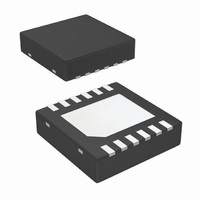
LM3553SD/NOPB National Semiconductor, LM3553SD/NOPB Datasheet - Page 9

LM3553SD/NOPB
Manufacturer Part Number
LM3553SD/NOPB
Description
IC LED DRIVER PHOTO FLASH 12-LLP
Manufacturer
National Semiconductor
Series
PowerWise®r
Type
Photo Flash LED (I²C Interface)r
Datasheet
1.LM3553SDNOPB.pdf
(18 pages)
Specifications of LM3553SD/NOPB
Topology
Step-Up (Boost)
Number Of Outputs
1
Internal Driver
Yes
Type - Primary
Backlight, Flash/Torch
Frequency
1MHz ~ 1.35MHz
Voltage - Supply
2.7 V ~ 5.5 V
Mounting Type
Surface Mount
Package / Case
12-LLP
Operating Temperature
-30°C ~ 85°C
Current - Output / Channel
1.2A
Internal Switch(s)
Yes
Efficiency
90%
Operating Supply Voltage (typ)
3.3/5V
Number Of Segments
2
Operating Temperature (min)
-30C
Operating Temperature (max)
85C
Operating Temperature Classification
Commercial
Package Type
LLP EP
Pin Count
12
Mounting
Surface Mount
Operating Supply Voltage (min)
2.7V
Operating Supply Voltage (max)
5.5V
For Use With
LM3553SDEV - BOARD EVALUATION FOR LM3553S
Lead Free Status / RoHS Status
Lead free / RoHS Compliant
Voltage - Output
-
Lead Free Status / Rohs Status
Compliant
Other names
LM3553SD
LM3553SD
LM3553SDTR
LM3553SD
LM3553SDTR
Connection Diagram
I
DATA VALIDITY
The data on SDA line must be stable during the HIGH period
of the clock signal (SCL). In other words, the state of the data
line can only be changed when CLK is LOW.
A pull-up resistor between VIO and SDA must be greater than
[ (VIO-V
Using a larger pull-up resistor results in lower switching cur-
rent with slower edges, while using a smaller pull-up results
in higher switching currents with faster edges.
2
C Compatible Interface
OL
) / 3.7mA] to meet the V
FIGURE 1. Data Validity Diagram
Typical System Configuration
OL
ack = acknowledge (SDA pulled down by the slave)
requirement on SDA.
20171433
id = chip address, 53h for LM3553
FIGURE 3. Write Cycle
20171404
w = write (SDA = "0")
9
START AND STOP CONDITIONS
START and STOP conditions classify the beginning and the
end of the I
signal transitioning from HIGH to LOW while SCL line is
HIGH. A STOP condition is defined as the SDA transitioning
from LOW to HIGH while SCL is HIGH. The I
generates START and STOP conditions. The I
sidered to be busy after a START condition and free after a
STOP condition. During data transmission, the I
can generate repeated START conditions. First START and
repeated START conditions are equivalent, function-wise.
The data on SDA line must be stable during the HIGH period
of the clock signal (SCL). In other words, the state of the data
line can only be changed when CLK is LOW.
TRANSFERRING DATA
Every byte put on the SDA line must be eight bits long, with
the most significant bit (MSB) being transferred first. Each
byte of data has to be followed by an acknowledge bit. The
acknowledge related clock pulse is generated by the master.
The master releases the SDA line (HIGH) during the acknowl-
edge clock pulse. The LM3553 pulls down the SDA line during
the 9th clock pulse, signifying an acknowledge. The LM3553
generates an acknowledge after each byte has been re-
ceived.
After the START condition, the I
dress. This address is seven bits long followed by an eighth
bit which is a data direction bit (R/W). The LM3553 address
is 53h. For the eighth bit, a “0” indicates a WRITE and a “1”
indicates a READ. The second byte selects the register to
which the data will be written. The third byte contains data to
write to the selected register.
FIGURE 2. Start and Stop Conditions
2
C session. A START condition is defined as SDA
2
C master sends a chip ad-
2
20171413
C master always
2
C bus is con-
www.national.com
2
C master
20171412


