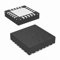
ISL97675IRZ-TK Intersil, ISL97675IRZ-TK Datasheet - Page 17

ISL97675IRZ-TK
Manufacturer Part Number
ISL97675IRZ-TK
Description
IC LED DVR PWM CTRL 4CH 20QFN
Manufacturer
Intersil
Type
Backlight, White LEDr
Datasheet
1.ISL97675IRZ-TK.pdf
(20 pages)
Specifications of ISL97675IRZ-TK
Topology
PWM, Step-Up (Boost)
Number Of Outputs
4
Internal Driver
Yes
Type - Primary
Backlight
Frequency
600kHz, 1.2MHz
Voltage - Supply
4.5 V ~ 26 V
Voltage - Output
45V
Mounting Type
Surface Mount
Package / Case
20-VQFN
Operating Temperature
-40°C ~ 85°C
Current - Output / Channel
30mA
Internal Switch(s)
Yes
Efficiency
92%
Lead Free Status / RoHS Status
Lead free / RoHS Compliant
Other names
ISL97675IRZ-TKTR
Components Selections
According to the inductor Voltage-Second Balance
principle, the change of inductor current during the
switching regulator On-time is equal to the change of
inductor current during the switching regulator Off-time.
Since the voltage across an inductor is:
and ΔI
where D is the switching duty cycle defined by the turn-on
time over the switching period. V
forward voltage which can be neglected for
approximation.
Rearranging the terms without accounting for V
the boost ratio and duty cycle respectively as:
CASE
V
(
V
D
V
L
O
10
11
5
6
7
8
9
I
=
–
⁄
=
V
(
0 ) L ⁄
V
L
I
L
=
O
FB1 LED Open
Circuit but has
paralleled Zener
FB1 LED Open
Circuit but has
paralleled Zener
FB1 LED Open
Circuit but has
paralleled Zener
Channel-to-Channel
ΔVF too high
Channel-to-Channel
ΔVF too high
Output LED stack
voltage too high
V
GND at start-up or
V
operation
×
@ T
FAILURE MODE
1
OUT
OUT
ΔI
–
×
⁄
V
L
(
D
1 D
I
/LX shorted to
⁄
ON
) V
shorted in
Δt
×
–
⁄
t
S
O
= ΔI
)
=
(
V
L
O
@ T
–
V
D
OFF
17
–
Upper OTP not triggered
and FB1 < 4V
Upper OTP triggered but
FB1 < 4V
Upper OTP not triggered
but FBx > 4V
Lower OTP triggered but
FBx < 4V
Upper OTP triggered but
FBx < 4V
V
LX current and timing are
monitored.
OVP pins monitored for
excursions below 20% of
OVP threshold.
OUT
V
, therefore:
I
DETECTION MODE
)
⁄
> VOVP
L
D
×
1 (
is Schottky diode
TABLE 3. PROTECTIONS TABLE (Continued)
–
D )
×
t
S
D
(EQ. 13)
(EQ. 14)
(EQ. 15)
(EQ. 16)
gives
FAILED CHANNEL ACTION
FB1 remains ON and has
highest VF, thus V
increases.
All channels go off until chip
cooled and then comes back
on with current reduced to
76%. Subsequent OTP
triggers will reduce I
further
FB1 remains ON and has
highest VF, thus V
increases.
Any channel at below the target current will fault out
after 6 PWM cycles.
Remaining channels driven with normal current.
All channels go off until chip cooled and then comes
back on with current reduced to 76%. Subsequent OTP
triggers will reduce I
Any channel that is below the target current will time-
out after 6 PWM cycles, and V
normal regulation voltage required for other channels.
The chip is permanently shutdown 31ms after
power-up if V
ISL97675
Input Capacitor
Switching regulators require input capacitors to deliver
peak charging current and to reduce the impedance of
the input supply. This reduces interaction between the
regulator and input supply, thereby improving system
stability. The high switching frequency of the loop causes
almost all ripple current to flow in the input capacitor,
which must be rated accordingly.
A capacitor with low internal series resistance should be
chosen to minimize heating effects and improve system
efficiency, such as X5R or X7R ceramic capacitors, which
offer small size and a lower value of temperature and
voltage coefficient compared to other ceramic capacitors.
In boost mode, input current flows continuously into the
inductor; AC ripple component is only proportional to the
rate of the inductor charging, thus, smaller value input
capacitors may be used. It is recommended that an input
capacitor of at least 10µF be used. Ensure the voltage
rating of the input capacitor is suitable to handle the full
supply range.
OUT
/Lx is shorted to GND.
OUT
OUT
OUT
OUT
further
OUT
FB2 through FB4 ON,
Q2 through Q4 burn
power
Same as FB1
V
FB-X switches OFF after
6 PWM cycles. This is an
unwanted shut off and
can be prevented by
setting OVP at an
appropriate level.
OUT
GOOD CHANNELS
will return to the
increases, then
ACTION
VF of FB1
VF of FB1
VF of FB1
Highest VF of
FB1 through FB4
Highest VF of
FB1 through FB4
Highest VF of
FB1 through FB4
REGULATED
V
May 19, 2010
BY
OUT
FN7630.0


