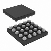
LP5526TL/NOPB National Semiconductor, LP5526TL/NOPB Datasheet - Page 8

LP5526TL/NOPB
Manufacturer Part Number
LP5526TL/NOPB
Description
IC LED DRVR WT/RGB BCKLT 25-USMD
Manufacturer
National Semiconductor
Series
PowerWise®r
Type
Backlight, White LED, RGB (I²C Interface)r
Datasheet
1.LP5526TLNOPB.pdf
(32 pages)
Specifications of LP5526TL/NOPB
Constant Current
Yes
Topology
PWM, Step-Up (Boost)
Number Of Outputs
5
Internal Driver
Yes
Type - Primary
Backlight, Light Management Unit (LMU)
Type - Secondary
RGB, White LED
Frequency
1MHz
Voltage - Supply
3 V ~ 5.5 V
Voltage - Output
8 V ~ 20 V
Mounting Type
Surface Mount
Package / Case
25-MicroSMD
Operating Temperature
-30°C ~ 85°C
Current - Output / Channel
150mA
Internal Switch(s)
Yes
Efficiency
88%
For Use With
LP5526TLEV - BOARD EVAL LP5526 LMU LED DRIVER
Lead Free Status / RoHS Status
Lead free / RoHS Compliant
Other names
LP5526TLTR
www.national.com
I
I
V
RDS
f
t
t
I
LOAD
LOAD
PWM
PULSE
STARTUP
MAX
OUT
Symbol
MAGNETIC BOOST DC/DC CONVERTER ELECTRICAL CHARACTERISTICS
Note: Maximum non-continuous currents rates as short pulses (t < 1s). Exposure to maximum rating conditions for extended periods may affect device reliability.
BOOST STANDBY MODE
User can set the Boost Converter to STANDBY mode by writ-
ing the register bit EN_BOOST low. When EN_BOOST is
written high, the converter starts for 20ms in low current PWM
mode and then goes to normal PWM mode. All LED outputs
are off during the 20ms delay to ensure smooth startup.
BOOST OUTPUT VOLTAGE CONTROL
User can control the boost output voltage by Boost Output 8-
bit register.
If register value is lower than 8, then value of 8 is used inter-
nally.
ON
0000 1000
0000 1001
0000 1010
0000 1011
0000 1100
0000 1101
0000 1110
0000 1111
0001 0000
0001 0001
0001 0010
0001 0011
0001 0100
Boost Output [7:0]
Bin
Register 0DH
Maximum Non-Continuous
Load Current
Maximum Continuous Load
Current
Output Voltage Accuracy
(FB Pin)
Switch ON Resistance
PWM Mode Switching
Frequency
Frequency Accuracy
Switch Pulse Minimum
Width
Startup Time
SW Pin Current Limit
Parameter
Dec
10
11
12
13
14
15
16
17
18
19
20
8
9
Voltage (typical)
Boost Output
10.0V
11.0V
12.0V
13.0V
14.0V
15.0V
16.0V
17.0V
18.0V
19.0V
20.0V
8.0V
9.0V
3.0V
V
3.2V < V
V
3.0V = V
V
3.0V
V
I
RT = 82 kΩ
RT = 82 kΩ
no load
Boost startup from STANDBY to V
20V, no load
SW
OUT
OUT
OUT
OUT
= 0.5A
≤
≤
= 20V
= 20V
= 20V
= 20V
V
V
IN
IN
IN
IN
≤
≤
3.2V
5.5V
Conditions
8
If register value is higher than 20, then value of 20 is used
internally.
OUT
Boost Output Voltage Control
=
−2.3
Min
-1.7
−7
−9
1500
0.15
Typ
1.0
45
15
1850
20179778
Max
+2.3
+1.7
140
150
100
0.3
+7
+9
Units
MHz
mA
mA
ms
ns
%
%
Ω


