LM3554TME/NOPB National Semiconductor, LM3554TME/NOPB Datasheet - Page 38
LM3554TME/NOPB
Manufacturer Part Number
LM3554TME/NOPB
Description
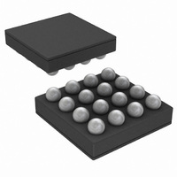
IC LED DVR PHOTO FLASH 16-USMD
Manufacturer
National Semiconductor
Type
Photo Flash LED (I²C Interface)r
Datasheet
1.LM3554TMENOPB.pdf
(40 pages)
Specifications of LM3554TME/NOPB
Constant Current
Yes
Topology
High Side, Step-Up (Boost)
Number Of Outputs
2
Internal Driver
Yes
Type - Primary
Flash/Torch
Type - Secondary
White LED
Frequency
2MHz
Voltage - Supply
2.7 V ~ 5.5 V
Voltage - Output
5V
Mounting Type
Surface Mount
Package / Case
16-MicroSMD
Operating Temperature
-30°C ~ 85°C
Current - Output / Channel
600mA
Internal Switch(s)
Yes
Efficiency
90%
Led Driver Application
LED Backlighting, Portable Electronics
No. Of Outputs
2
Output Current
1.2A
Input Voltage
2.7V To 5.5V
Dimming Control Type
I2C
Rohs Compliant
Yes
Lead Free Status / RoHS Status
Lead free / RoHS Compliant
Other names
LM3554TMETR


www.national.com
Layout Recommendations
The high frequency and large switching currents of the
LM3554 make the choice of layout important. The following
steps should be used as a reference to ensure the device is
stable and maintains proper voltage and current regulation
across its intended operating voltage and current range.
1.
2.
3.
Place C
and as close to the device as possible. The input
capacitor conducts the driver currents during the low-
side MOSFET turn-on and turn-off and can see current
spikes over 1A in amplitude. Connecting the input
capacitor through short wide traces on both the IN and
GND terminals will reduce the inductive voltage spikes
that occur during switching and which can corrupt the
V
Place C
and as close as possible to the OUT and GND terminal.
The returns for both C
at one point, and as close to the GND pin as possible.
Connecting C
the series inductance on the OUT and GND terminals
that can corrupt the V
excessive noise in the device and surrounding circuitry.
Connect the inductor on the top layer close to the SW pin.
There should be a low impedance connection from the
inductor to SW due to the large DC inductor current, and
at the same time the area occupied by the SW node
should be small so as to reduce the capacitive coupling
of the high dV/dt present at SW that can couple into
nearby traces.
IN
line.
OUT
IN
on the top layer (same layer as the LM3554)
on the top layer (same layer as the LM3554)
OUT
through short wide traces will reduce
OUT
IN
and C
and GND line and cause
OUT
should come together
38
4.
5.
6.
Avoid routing logic traces near the SW node so as to
avoid any capacitively coupled voltages from SW onto
any high-impedance logic lines such as TX1/TORCH/
GPIO1, ENVM/TX2/GPIO2, HWEN, LEDI/NTC (NTC
mode), SDA, and SCL. A good approach is to insert an
inner layer GND plane underneath the SW node and
between any nearby routed traces. This creates a shield
from the electric field generated at SW.
Terminate the Flash LED cathodes directly to the GND
pin of the LM3554. If possible, route the LED returns with
a dedicated path so as to keep the high amplitude LED
currents out the GND plane. For Flash LEDs that are
routed relatively far away from the LM3554, a good
approach is to sandwich the forward and return current
paths over the top of each other on two layers. This will
help in reducing the inductance of the LED current paths.
The NTC Thermistor is intended to have its return path
connected to the LED's cathode. This allows the
thermistor resistive divider voltage (V
comparators threshold as V
thermistor-to-LED cathode junction can have low thermal
resistivity since both the LED and the thermistor are
electrically connected at GND. The drawback is that the
thermistor's return will see the switching currents from
the LM3554's boost converter. Because of this, it is
necessary to have a filter capacitor at the NTC pin which
terminates close to the GND of the LM3554 and which
can conduct the switched currents to GND.
NTC
is falling. Additionally, the
NTC
) to trip the
Related parts for LM3554TME/NOPB
Image
Part Number
Description
Manufacturer
Datasheet
Request
R

Part Number:
Description:
LM3554 PRODUCT BRIEF Synchronous Boost Converter with 1.2A Dual High Side LED Drivers and I<sup>2</sup>C Compatible Interface; Package: MICRO SMD; No of Pins: 16; Qty per Container: 250/Reel
Manufacturer:
National Semiconductor
Part Number:
Description:
National Semiconductor [8-Bit D/A Converter]
Manufacturer:
National Semiconductor
Datasheet:
Part Number:
Description:
National Semiconductor [Media Coprocessor]
Manufacturer:
National Semiconductor
Datasheet:
Part Number:
Description:
Digitally Controlled Tone and Volume Circuit with Stereo Audio Power Amplifier, Microphone Preamp Stage and National 3D Sound
Manufacturer:
National Semiconductor
Datasheet:
Part Number:
Description:
Digitally Controlled Tone and Volume Circuit with Stereo Audio Power Amplifier, Microphone Preamp Stage and National 3D Sound
Manufacturer:
National Semiconductor
Datasheet:
Part Number:
Description:
AC97 Rev 2 Codec with Sample Rate Conversion and National 3D Sound
Manufacturer:
National Semiconductor
Part Number:
Description:
Manufacturer:
National Semiconductor
Datasheet:
Part Number:
Description:
Manufacturer:
National Semiconductor
Datasheet:
Part Number:
Description:
General Purpose, Low Voltage, Low Power, Rail-to-Rail Output Operational Amplifiers
Manufacturer:
National Semiconductor
Datasheet:
Part Number:
Description:
8-bit 20 MSPS flash A/D converter.
Manufacturer:
National Semiconductor
Datasheet:
Part Number:
Description:
Low Noise Quad Operational Amplifier
Manufacturer:
National Semiconductor
Datasheet:
Part Number:
Description:
Quad Differential Line Receivers
Manufacturer:
National Semiconductor
Datasheet:
Part Number:
Description:
Quad High Speed Trapezoidal? Bus Transceiver
Manufacturer:
National Semiconductor
Datasheet:
Part Number:
Description:
Dual Line Receiver
Manufacturer:
National Semiconductor
Datasheet: