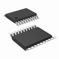
LM3424MH/NOPB National Semiconductor, LM3424MH/NOPB Datasheet - Page 18

LM3424MH/NOPB
Manufacturer Part Number
LM3424MH/NOPB
Description
IC LED DVR BUCK/BOOST 20-TSSOP
Manufacturer
National Semiconductor
Series
PowerWise®r
Type
High Power, Constant Currentr
Datasheet
1.LM3424MHNOPB.pdf
(50 pages)
Specifications of LM3424MH/NOPB
Constant Current
Yes
Topology
Flyback, PWM, SEPIC, Step-Down (Buck), Step-Up (Boost)
Number Of Outputs
1
Internal Driver
No
Type - Primary
Automotive
Type - Secondary
High Brightness LED (HBLED)
Frequency
2MHz
Voltage - Supply
4.5 V ~ 75 V
Mounting Type
Surface Mount
Package / Case
20-TSSOP Exposed Pad, 20-eTSSOP, 20-HTSSOP
Operating Temperature
-40°C ~ 125°C
Current - Output / Channel
1A
Internal Switch(s)
Yes
Efficiency
96%
Lead Free Status / RoHS Status
Lead free / RoHS Compliant
Voltage - Output
-
Other names
LM3424MH
www.national.com
Then COMP will clamp to SS, forcing COMP to rise (the last
200 mV before switching begins) according to the C
ing time (t
The system start-up time (t
C
C
As a general rule of thumb, standard smooth startup operation
can be achieved with C
OVER-VOLTAGE LOCKOUT (OVLO)
The LM3424 can be configured to detect an output (or input)
over-voltage condition via the OVP pin. The pin features a
precision 1.24V threshold with 20 µA (typical) of hysteresis
current as shown in
exceeded, the GATE pin is immediately pulled low and a 20
µA current source provides hysteresis to the lower threshold
of the OVLO hysteretic band.
If the LEDs are referenced to a potential other than ground
(floating), as in the buck-boost and buck configuration, the
output voltage (V
ground by using a single PNP as shown in
The over-voltage turn-off threshold (V
Ground Referenced
Floating
In the ground referenced configuration, the voltage across
R
V
The over-voltage hysteresis (V
SS
SS
OV2
O
- 620 mV where 620 mV approximates V
< 0.4 x C
> 0.4 x C
is V
FIGURE 13. Over-Voltage Protection Circuitry
O
SS
- 1.24V whereas in the floating configuration it is
) which can be estimated as:
CMP
CMP
O
) should be sensed and translated to
Figure
SS
= C
SU
13. When the OVLO threshold is
or t
CMP
HYSO
SU-SS
.
) is defined:
TURN-OFF
) is defined as:
Figure
BE
) is defined:
of the PNP.
14.
SS
30085758
charg-
18
INPUT UNDER-VOLTAGE LOCKOUT (UVLO)
The nDIM pin is a dual-function input that features an accurate
1.24V threshold with programmable hysteresis as shown in
Figure
for the LEDs and as a V
and exceeds the 1.24V threshold, 20 µA (typical) of current is
driven out of the nDIM pin into the resistor divider providing
programmable hysteresis.
When using the nDIM pin for UVLO and PWM dimming con-
currently, the UVLO circuit can have an extra series resistor
to set the hysteresis. This allows the standard resistor divider
to have smaller resistor values minimizing PWM delays due
to a pull-down MosFET at the nDIM pin (see PWM Dimming
section). In general, at least 3V of hysteresis is preferable
when PWM dimming, if operating near the UVLO threshold.
The turn-on threshold (V
The hysteresis (V
UVLO only
PWM dimming and UVLO
15. This pin functions as both the PWM dimming input
FIGURE 14. Floating Output OVP Circuitry
FIGURE 15. UVLO Circuit
HYS
) is defined as follows:
IN
TURN-ON
UVLO. When the pin voltage rises
) is defined as follows:
30085759
300857a5


