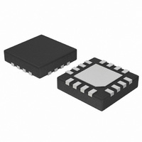
CAT3647HV3-GT2 ON Semiconductor, CAT3647HV3-GT2 Datasheet

CAT3647HV3-GT2
Specifications of CAT3647HV3-GT2
Available stocks
Related parts for CAT3647HV3-GT2
CAT3647HV3-GT2 Summary of contents
Page 1
... LED3 C2+ NC C1− RSET C1+ (Top View) MARKING DIAGRAM JAAP AXXX YWW JAAP = CAT3647HV3−GT2 A = Assembly Location XXX = Last Three Digits of Assembly Lot Number Y = Production Year (Last Digit Production Week (Two Digits) ORDERING INFORMATION Device Package Shipping TQFN−16 2,000/ CAT3647HV3−GT2 (Note 1) (Pb− ...
Page 2
5.5 V 1−Wire EZDimt Programming 3.74 kΩ Table 1. ABSOLUTE MAXIMUM RATINGS VIN, LEDx, C1±, C2±, EN/DIM, RSET voltage VOUT voltage Storage Temperature Range Junction Temperature Range Stresses exceeding Maximum Ratings may damage the device. ...
Page 3
Table 3. ELECTRICAL OPERATING CHARACTERISTICS (over recommended operating conditions unless specified otherwise) V Symbol Name I Quiescent Current Q I Shutdown Current QSHDN I LED Current Setting LED-ACC I LED Current Accuracy LED-ACC I LED Channel Matching LED-DEV V RSET ...
Page 4
Table 4. RECOMMENDED EN/DIM TIMING (For 2.4 V ≤ V ≤ 5.5 V, over full ambient temperature range -40°C to +85°C.) IN Symbol Name T EN/DIM program low time LO T EN/DIM program high time HI T EN/DIM low time ...
Page 5
TYPICAL PERFORMANCE CHARACTERISTICS ( LEDs OUT 100 V = 3.3 V 1.33x 4.5 4.0 3.5 3.0 INPUT VOLTAGE ...
Page 6
TYPICAL PERFORMANCE CHARACTERISTICS ( LEDs OUT 1.3 1.2 1.5x Mode 1.1 1.0 0.9 1.33x, 2x Mode 0.8 0.7 − TEMPERATURE (°C) Figure 9. Switching Frequency ...
Page 7
TYPICAL PERFORMANCE CHARACTERISTICS ( LEDs OUT Figure 15. Power Up Delay (1x Mode) Figure 17. Operating Waveforms in 1x Mode Figure 19. Switching Waveforms in 1.5x Mode ...
Page 8
TYPICAL PERFORMANCE CHARACTERISTICS ( LEDs OUT 4.0 1x Mode 3.5 3.0 2.5 2.0 1.5 1.0 0 100 200 OUTPUT CURRENT (mA) Figure 21. Foldback Current ...
Page 9
Table 6. PIN DESCRIPTION Name LED1 LED1 cathode terminal. LED2 LED2 cathode terminal. LED3 LED3 cathode terminal. RSET Connect resistor RSET to set the LED current. EN/DIM Device enable (active high) and Dimming Control. VOUT Charge pump output connected to ...
Page 10
Block Diagram VIN EN/DIM 100 kΩ Serial Interface Registers Figure 24. CAT3647 Functional Block Diagram Basic Operation At power-up, the CAT3647 starts operating in 1x mode where the output will be approximately equal to the input supply voltage (less any ...
Page 11
LED Current Selection After power-up, the LED current is set by the external resistor (R ) value and the number of pulses (n) on the SET EN/DIM input as follows: 0.6 V LED current + 125 R SET The full ...
Page 12
Unused LED Channels For applications not requiring all the channels recommended the unused LED pins be tied directly to VOUT (see Figure 26 C1+ C1− C2+ C2− VIN VOUT C 2.4 V ...
Page 13
D PIN#1 INDEX AREA TOP VIEW SYMBOL MIN NOM A 0.70 0.75 A1 0.00 0.02 A3 0.20 REF b 0.18 0.25 D 2.90 3.00 D2 1.40 −−− E 2.90 3.00 E2 1.40 −−− e 0.50 BSC L 0.30 0.40 Notes: ...
Page 14
... All packages are RoHS−compliant (Lead−free, Halogen−free). 3. The standard lead finish is NiPdAu. 4. The device used in the above example is a CAT3647HV3−GT2 (TQFN, NiPdAu, Tape & Reel, 2,000/Reel). 5. For additional package and temperature options, please contact your nearest ON Semiconductor Sales office. ...


