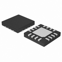
CAT3604VHV4-GT2 ON Semiconductor, CAT3604VHV4-GT2 Datasheet - Page 11

CAT3604VHV4-GT2
Manufacturer Part Number
CAT3604VHV4-GT2
Description
IC LED DRVR WT/CLR BCKLGT 16TQFN
Manufacturer
ON Semiconductor
Series
QUAD-Mode®r
Type
Backlight, White LED, Color LEDr
Datasheet
1.CAT3604VHV4-GT2.pdf
(14 pages)
Specifications of CAT3604VHV4-GT2
Topology
PWM, Switched Capacitor (Charge Pump)
Number Of Outputs
4
Internal Driver
Yes
Type - Primary
Backlight
Type - Secondary
White LED
Frequency
800kHz ~ 1.3MHz
Voltage - Supply
2.5 V ~ 5.5 V
Mounting Type
Surface Mount
Package / Case
16-TFQFN Exposed Pad
Operating Temperature
-40°C ~ 85°C
Current - Output / Channel
30mA
Internal Switch(s)
Yes
Efficiency
92%
Number Of Segments
3
Operating Supply Voltage
2.7 V to 5.5 V
Maximum Supply Current
30000 uA (Typ)
Maximum Operating Temperature
+ 85 C
Mounting Style
SMD/SMT
Minimum Operating Temperature
- 40 C
Operating Supply Voltage (typ)
3.3/5V
Operating Temperature (min)
-40C
Operating Temperature (max)
85C
Operating Temperature Classification
Industrial
Package Type
TQFN EP
Pin Count
16
Mounting
Surface Mount
Operating Supply Voltage (min)
2.5V
Operating Supply Voltage (max)
5.5V
Lead Free Status / RoHS Status
Lead free / RoHS Compliant
Voltage - Output
-
Lead Free Status / Rohs Status
Lead free / RoHS Compliant
Other names
CAT3604VHV4-GT2TR
Available stocks
Company
Part Number
Manufacturer
Quantity
Price
Part Number:
CAT3604VHV4-GT2
Manufacturer:
ON/安森美
Quantity:
20 000
device runs diagnostics and goes to 1x mode where the
output is basically equal to the input voltage.
itself and reevaluate the mode.
a thermal protection shutdown mode. When the device
temperature drops to about +130°C, the device resumes
normal operation.
LED Selection
4.3 V may be used. Selecting LEDs with lower V
recommended in order to extend battery life and keep the
driver in 1x mode longer as the battery voltage decreases.
3.5 V V
supply voltage of 0.2 V.
External Components
for decoupling input, output, and for the charge pump. Both
capacitors type X5R and X7R are recommended for the
LED driver application. In all charge pump modes, the input
current ripple is kept very low by design and an input bypass
capacitor of 1 mF is sufficient.
not introduce switching noise back onto the supply.
Recommended Layout
high frequency. It is recommended to minimize trace length
to all four capacitors. A ground plane should cover the area
under the driver IC as well as the bypass capacitors. Short
connection to ground on capacitors C
implemented with the use of multiple via. A copper area
matching the TQFN exposed pad (TAB) must be connected
to the ground plane underneath. The use of multiple via
improves the package heat dissipation.
As soon as the output exceeds about 6 V, the driver resets
If the die temperature reaches +150°C, the device enters
LEDs with forward voltages (V
For example, if a 3.3 V V
The driver requires four external 1 mF ceramic capacitors
In 1x mode, the device operates in linear mode and does
In charge pump mode, the driver switches internally at a
F
LED, the driver will stay in 1x mode for a lower
Figure 27. PCB Layout
F
LED is selected instead of a
F
) ranging from 1.3 V to
IN
and C
OUT
http://onsemi.com
can be
F
is
11
PWM Dimming
as well as High Resolution PWM dimming control on the
LED Channels.
held low for 1.5 ms. During the “soft−start” power−up
sequence from the shutdown mode, the LED current
typically settles within 40 ms (for 1X mode operation). This
LED current settling time becomes 400 ms if 1.33X
operation is needed (i.e low battery voltage).
frequencies at 2 kHz or above), the device will remain
powered and only the LED channels output will be switched
on and off during the PWM (the rest of the device will
remain powered−up). This allows the output channels to
have “instant−on” response, where the LED current settles
within 1 ms of the applied PWM dimming signals. This
“instant−on” modes makes the device suitable for extremely
high frequency PWM dimming schemes.
up to 100 kHz and with duty cycles of 30% and 70%.
should meet the following timing limits:
•
•
The EN pin is used to provide total Shutdown of the device
Shutdown of the device occurs after the EN pin has been
For High Resolution PWM dimming control (typically
Figure 28 shows the output current for PWM frequencies
For best performance, the duty cycle off−time T
for slow frequency ≤ 600 Hz, T
for fast frequency ≥ 1 kHz, T
100
90
80
70
60
50
40
30
20
10
Figure 28. Output Current vs. PWM Frequency
0.1
30% DC
70% DC
PWM FREQUENCY (kHz)
1
OFF
OFF
≤ 400 ms
≥ 800 ms
10
100
OFF


