CAT3604VHV4-GT2 ON Semiconductor, CAT3604VHV4-GT2 Datasheet - Page 9
CAT3604VHV4-GT2
Manufacturer Part Number
CAT3604VHV4-GT2
Description
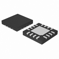
IC LED DRVR WT/CLR BCKLGT 16TQFN
Manufacturer
ON Semiconductor
Series
QUAD-Mode®r
Type
Backlight, White LED, Color LEDr
Datasheet
1.CAT3604VHV4-GT2.pdf
(14 pages)
Specifications of CAT3604VHV4-GT2
Topology
PWM, Switched Capacitor (Charge Pump)
Number Of Outputs
4
Internal Driver
Yes
Type - Primary
Backlight
Type - Secondary
White LED
Frequency
800kHz ~ 1.3MHz
Voltage - Supply
2.5 V ~ 5.5 V
Mounting Type
Surface Mount
Package / Case
16-TFQFN Exposed Pad
Operating Temperature
-40°C ~ 85°C
Current - Output / Channel
30mA
Internal Switch(s)
Yes
Efficiency
92%
Number Of Segments
3
Operating Supply Voltage
2.7 V to 5.5 V
Maximum Supply Current
30000 uA (Typ)
Maximum Operating Temperature
+ 85 C
Mounting Style
SMD/SMT
Minimum Operating Temperature
- 40 C
Operating Supply Voltage (typ)
3.3/5V
Operating Temperature (min)
-40C
Operating Temperature (max)
85C
Operating Temperature Classification
Industrial
Package Type
TQFN EP
Pin Count
16
Mounting
Surface Mount
Operating Supply Voltage (min)
2.5V
Operating Supply Voltage (max)
5.5V
Lead Free Status / RoHS Status
Lead free / RoHS Compliant
Voltage - Output
-
Lead Free Status / Rohs Status
Lead free / RoHS Compliant
Other names
CAT3604VHV4-GT2TR
Available stocks
Company
Part Number
Manufacturer
Quantity
Price

Part Number:
CAT3604VHV4-GT2
Manufacturer:
ON/安森美
Quantity:
20 000


Pin Function
VIN is the supply pin for the charge pump. A small 1 mF
ceramic bypass capacitor is required between the VIN pin
and ground near the device. The operating input voltage
range is from 2.5 V to 5.5 V. Whenever the input supply falls
below the under−voltage threshold (1.8 V), all the LED
channels are disabled and the device enters shutdown mode.
EN is the enable input and the high resolution PWM
dimming control. Levels of logic high and logic low are set
at 1.3 V and 0.4 V respectively. When EN is initially taken
high, the device becomes enabled and all LED currents are
set according to the R
“zero current” shutdown mode, the EN pin must be held low
for at least 1.5 ms.
VOUT is the charge pump output that is connected to the
LED anodes. A small 1 mF ceramic bypass capacitor is
required between the V
GND is the ground reference for the charge pump. The pin
must be connected to the ground plane on the PCB.
Table 6. PIN DESCRIPTION
Pin #
TAB
10
12
13
14
15
16
11
1
2
3
4
5
6
7
8
9
Name
VOUT
RSET
LED4
LED3
LED2
LED1
GND
GND
C1+
C2+
C1−
C2−
VIN
EN
NC
NC
NC
SET
OUT
Device enable (active high).
Not connected inside the package.
Not connected inside the package.
Not connected inside the package.
Connect resistor RSET to set the LED current.
Charge pump output connected to the LED anodes.
Charge pump input, connect to battery or supply.
Bucket capacitor 1 Positive terminal
Bucket capacitor 1 Negative terminal
Bucket capacitor 2 Negative terminal
Bucket capacitor 2 Positive terminal
Ground Reference
LED4 cathode terminal.
LED3 cathode terminal.
LED2 cathode terminal.
LED1 cathode terminal.
Connect to GND on the PCB.
resistor. To place the device into
pin and ground near the device.
http://onsemi.com
9
C1+, C1− are connected to each side of the ceramic bucket
capacitor C
C2+, C2− are connected to each side of the ceramic bucket
capacitor C
LED1 to LED4 provide the internal regulated current
source for each of the LED cathodes. These pins enter
high−impedance zero current state whenever the device is
placed in shutdown mode. If an LED pin is directly tied to
VOUT, that channel is disabled.
TAB is the exposed pad underneath the package. For best
thermal performance, the tab should be soldered to the PCB
and connected to the ground plane.
RSET is connected to the resistor (R
for the LEDs. The voltage at this pin regulated to 0.6 V. The
ground side of the external resistor should be star connected
back to the GND of the PCB. In shutdown mode, RSET
becomes high impedance.
Function
1
2
.
.
SET
) to set the current
Related parts for CAT3604VHV4-GT2
Image
Part Number
Description
Manufacturer
Datasheet
Request
R

Part Number:
Description:
ON Semiconductor [VOLTAGE REGULATOR]
Manufacturer:
ON Semiconductor
Datasheet:
Part Number:
Description:
357-036-542-201 CARDEDGE 36POS DL .156 BLK LOPRO
Manufacturer:
ON Semiconductor
Datasheet:
Part Number:
Description:
357-036-542-201 CARDEDGE 36POS DL .156 BLK LOPRO
Manufacturer:
ON Semiconductor
Datasheet:
Part Number:
Description:
357-036-542-201 CARDEDGE 36POS DL .156 BLK LOPRO
Manufacturer:
ON Semiconductor
Datasheet:
Part Number:
Description:
357-036-542-201 CARDEDGE 36POS DL .156 BLK LOPRO
Manufacturer:
ON Semiconductor
Datasheet:
Part Number:
Description:
357-036-542-201 CARDEDGE 36POS DL .156 BLK LOPRO
Manufacturer:
ON Semiconductor
Datasheet:
Part Number:
Description:
357-036-542-201 CARDEDGE 36POS DL .156 BLK LOPRO
Manufacturer:
ON Semiconductor
Datasheet:
Part Number:
Description:
357-036-542-201 CARDEDGE 36POS DL .156 BLK LOPRO
Manufacturer:
ON Semiconductor
Datasheet:
Part Number:
Description:
357-036-542-201 CARDEDGE 36POS DL .156 BLK LOPRO
Manufacturer:
ON Semiconductor
Datasheet:
Part Number:
Description:
357-036-542-201 CARDEDGE 36POS DL .156 BLK LOPRO
Manufacturer:
ON Semiconductor
Datasheet:
Part Number:
Description:
357-036-542-201 CARDEDGE 36POS DL .156 BLK LOPRO
Manufacturer:
ON Semiconductor
Datasheet:
Part Number:
Description:
Manufacturer:
ON Semiconductor
Datasheet:
Part Number:
Description:
Manufacturer:
ON Semiconductor
Datasheet:
Part Number:
Description:
Manufacturer:
ON Semiconductor
Datasheet: