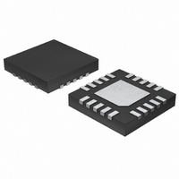
MAX8790ETP+ Maxim Integrated Products, MAX8790ETP+ Datasheet - Page 13

MAX8790ETP+
Manufacturer Part Number
MAX8790ETP+
Description
IC LED DRVR WHITE BCKLGT 20-TQFN
Manufacturer
Maxim Integrated Products
Type
Backlight, White LEDr
Datasheet
1.MAX8790ETP.pdf
(24 pages)
Specifications of MAX8790ETP+
Topology
PWM, Step-Up (Boost)
Number Of Outputs
6
Internal Driver
No
Type - Primary
Backlight
Type - Secondary
White LED
Frequency
1MHz
Voltage - Supply
4.5 V ~ 5.5 V, 5.5 V ~ 26 V
Voltage - Output
5V
Mounting Type
Surface Mount
Package / Case
20-TQFN Exposed Pad
Operating Temperature
-40°C ~ 85°C
Current - Output / Channel
25mA
Internal Switch(s)
Yes
Low Level Output Current
1000000 uA (Typ)
High Level Output Current
25.75 mA
Operating Supply Voltage
4.5 V to 26 V
Maximum Supply Current
2 mA
Maximum Power Dissipation
1349 mW
Maximum Operating Temperature
+ 85 C
Mounting Style
SMD/SMT
Minimum Operating Temperature
- 40 C
Lead Free Status / RoHS Status
Lead free / RoHS Compliant
Efficiency
-
Lead Free Status / Rohs Status
Lead free / RoHS Compliant
Table 1. Frequency Selection
At startup, the MAX8790 checks each FB_ pin to deter-
mine if the respective current string is enabled. Each
FB_ pin is internally pulled up with a 10µA current
source. If an FB_ pin is connected to GND, the corre-
sponding string current source is disabled. This feed-
back scan takes approximately 264µs, after which the
step-up converter begins switching.
When the SHDN pin is less than 0.8V, the MAX8790
shuts down the internal LDO, the reference, current
sources, and all control circuitry. The resulting supply
current is less than 10µA. While the n-channel MOSFET
is turned off, the step-up regulator’s output is connected
to IN through the external inductor and rectifier diode.
A tri-level OSC input sets the internal oscillator frequency
for the step-up converter, as shown in Table 1. High-fre-
quency (1MHz) operation optimizes the regulator for the
smallest component size, at the expense of efficiency
due to increased switching losses. Low-frequency
(500kHz) operation offers the best overall efficiency, but
requires larger components and PCB area.
To protect the step-up converter when the load is open,
or the output voltage becomes excessive for any rea-
son, the MAX8790 features a dedicated overvoltage
feedback input (OV). The OV pin is connected to the
center tap of a resistive voltage-divider from the high-
voltage output (see Figure 1). When the MAX8790 is
powered up, if none of the LED strings on FB1–FB6 are
connected to the step-up converter output, the step-up
converter regulates the output voltage to V
1.23V(1 + R1 / R2). When V
parator turns off N1. The step-up converter switch is
reenabled after the output voltage drops below the pro-
tection threshold.
Maintaining uniform LED brightness and dimming
capability are critical for LCD backlight applications.
The MAX8790 is equipped with a bank of six matched
current sources. These specialized current sources are
accurate to within ±1.5% and can be switched on and
Open
OSC
GND
V
Current Balancing for LCD Panel Applications
CC
______________________________________________________________________________________
SWITCHING FREQUENCY (kHz)
Six-String White LED Driver with Active
Overvoltage Protection
OV
LED Current Sources
Frequency Selection
exceeds 1.23V, a com-
1000
500
750
Shutdown
Startup
OUT
=
off within 10µs, enabling PWM frequencies of up to
2kHz. All LED full-scale currents are identical and are
set through the ISET pin (15mA < I
The minimum voltage drop across each current source
is approximately 450mV at 20mA. The low voltage drop
helps reduce dissipation while maintaining sufficient
compliance to control the LED current within the
required tolerances.
The LED current sources can be disabled by grounding
the respective FB_ pin at startup. When the IC is pow-
ered up, the controller scans settings for all FB_ pins. If
an FB_ pin is not grounded, an internal circuit pulls this
pin high, and the controller enables the corresponding
current source to regulate the string current. If the FB_ pin
is grounded, the controller disables the corresponding
current regulator. The current regulator cannot be dis-
abled by grounding any of the FB_ pins after the IC is
powered up.
All FB_ pins in use are measured and the highest signal
(HVC) and the lowest signal (LVC) are extracted for two
feedback loops. HVC is used to identify excessive dis-
sipation across the current-source inputs. When HVC is
greater than V
(see the Current-Source Fault Protection section), a
fault latch is set and the MAX8790 is shut down. The
LDO output is not affected by the fault latch. LVC is fed
into the step-up converter’s error amplifier to regulate
the step-up converter’s output voltage.
The LED current sources are protected against string
open, short, and gross mismatch faults, using overvolt-
age detection circuitry on each FB_ pin. If any of these
three fault conditions persists for a preset duration, the
MAX8790 is latched off. The duration of the fault time
depends on the dimming mode and the duty cycle of
the BRT input (D
interval is:
In analog dimming mode, the fault time is fixed at 65ms
for D
12.5%, the timeout interval is:
The fault latch can be cleared by cycling the power or
toggling the shutdown pin SHDN.
The MAX8790 step-up converter output voltage is regu-
lated according to the minimum value of the enable FB_
voltages. If an individual LED string is open, the respec-
tive FB_ is pulled down to near ground. In this situation,
the step-up converter output voltage increases but is
BRT
greater than 12.5%. When D
t
TIMEOUT_ANALOG
t
TIMEOUT_DPWM
Current-Source Fault Protection
CC
BRT
+ 0.6V (typ) for greater than 65ms
). In the DPWM mode, the timeout
Open-Current Source Protection
= 8.125ms/D
= 65ms/D
LED
< 25mA).
BRT
BRT
BRT
is less than
13


