MAX8790ETP+ Maxim Integrated Products, MAX8790ETP+ Datasheet - Page 21
MAX8790ETP+
Manufacturer Part Number
MAX8790ETP+
Description
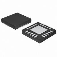
IC LED DRVR WHITE BCKLGT 20-TQFN
Manufacturer
Maxim Integrated Products
Type
Backlight, White LEDr
Datasheet
1.MAX8790ETP.pdf
(24 pages)
Specifications of MAX8790ETP+
Topology
PWM, Step-Up (Boost)
Number Of Outputs
6
Internal Driver
No
Type - Primary
Backlight
Type - Secondary
White LED
Frequency
1MHz
Voltage - Supply
4.5 V ~ 5.5 V, 5.5 V ~ 26 V
Voltage - Output
5V
Mounting Type
Surface Mount
Package / Case
20-TQFN Exposed Pad
Operating Temperature
-40°C ~ 85°C
Current - Output / Channel
25mA
Internal Switch(s)
Yes
Low Level Output Current
1000000 uA (Typ)
High Level Output Current
25.75 mA
Operating Supply Voltage
4.5 V to 26 V
Maximum Supply Current
2 mA
Maximum Power Dissipation
1349 mW
Maximum Operating Temperature
+ 85 C
Mounting Style
SMD/SMT
Minimum Operating Temperature
- 40 C
Lead Free Status / RoHS Status
Lead free / RoHS Compliant
Efficiency
-
Lead Free Status / Rohs Status
Lead free / RoHS Compliant


Careful PCB layout is important for proper operation. Use
the following guidelines for good PCB layout:
1) Minimize the area of the high current-switching loop
2) Connect high-current input and output components
3) Create a ground island (PGND) consisting of the
Figure 6. Startup Circuit with Large Capacitors on LED Strings
of the rectifier diode, external MOSFET, sense resis-
tor, and output capacitor to avoid excessive switching
noise. Use wide and short traces for the gate-drive
loop from the EXT pin, to the MOSFET gate, and
through the current-sense resistor, then returning to
the IC GND pin.
with short and wide connections. The high-current
input loop goes from the positive terminal of the input
capacitor to the inductor, to the external MOSFET,
then to the current-sense resistor, and to the input
capacitor’s negative terminal. The high-current out-
put loop is from the positive terminal of the input
capacitor to the inductor, to the rectifier diode, to
the positive terminal of the output capacitors,
reconnecting between the output capacitor and
input capacitor ground terminals. Avoid using vias
in the high-current paths. If vias are unavoidable,
use multiple vias in parallel to reduce resistance
and inductance.
input and output capacitor ground and negative ter-
minal of the current-sense resistor. Connect all
these together with short, wide traces or a small
Current Balancing for LCD Panel Applications
V
IN
SHDN
MAX8790
______________________________________________________________________________________
Six-String White LED Driver with Active
L1
EXT
FB2
FB3
FB4
FB5
FB6
FB1
PCB Layout Guidelines
N1
TO V
D1
C
OUT
IN
V
1MΩ
OUT
4) Place the overvoltage detection-divider resistors as
5) Place the IN pin bypass capacitor as close to the
6) Minimize the size of the LX node while keeping it
7) Refer to the MAX8790 evaluation kit for an example
ground plane. Maximizing the width of the power
ground traces improves efficiency and reduces out-
put-voltage ripple and noise spikes. Create an ana-
log ground island (AGND) consisting of the
overvoltage detection-divider ground connection,
the ISET and FSET resistor connections, CCV and
CPLL capacitor connections, and the device’s
exposed backside pad. Connect the AGND and
PGND islands by connecting the GND pins directly
to the exposed backside pad. Make no other con-
nections between these separate ground planes.
close to the OV pin as possible. The divider’s cen-
ter trace should be kept short. Placing the resistors
far away causes the sensing trace to become
antennas that can pick up switching noise. Avoid
running the sensing traces near LX.
device as possible. The ground connection of the
IN bypass capacitor should be connected directly
to GND pins with a wide trace.
wide and short. Keep the LX node away from the
feedback node and ground. If possible, avoid run-
ning the LX node from one side of the PCB to the
other. Use DC traces as shields, if necessary.
of proper board layout.
C
LED
21
Related parts for MAX8790ETP+
Image
Part Number
Description
Manufacturer
Datasheet
Request
R

Part Number:
Description:
MAX7528KCWPMaxim Integrated Products [CMOS Dual 8-Bit Buffered Multiplying DACs]
Manufacturer:
Maxim Integrated Products
Datasheet:
Part Number:
Description:
Single +5V, fully integrated, 1.25Gbps laser diode driver.
Manufacturer:
Maxim Integrated Products
Datasheet:
Part Number:
Description:
Single +5V, fully integrated, 155Mbps laser diode driver.
Manufacturer:
Maxim Integrated Products
Datasheet:
Part Number:
Description:
VRD11/VRD10, K8 Rev F 2/3/4-Phase PWM Controllers with Integrated Dual MOSFET Drivers
Manufacturer:
Maxim Integrated Products
Datasheet:
Part Number:
Description:
Highly Integrated Level 2 SMBus Battery Chargers
Manufacturer:
Maxim Integrated Products
Datasheet:
Part Number:
Description:
Current Monitor and Accumulator with Integrated Sense Resistor; ; Temperature Range: -40°C to +85°C
Manufacturer:
Maxim Integrated Products
Part Number:
Description:
TSSOP 14/A�/RS-485 Transceivers with Integrated 100O/120O Termination Resis
Manufacturer:
Maxim Integrated Products
Part Number:
Description:
TSSOP 14/A�/RS-485 Transceivers with Integrated 100O/120O Termination Resis
Manufacturer:
Maxim Integrated Products
Part Number:
Description:
QFN 16/A�/AC-DC and DC-DC Peak-Current-Mode Converters with Integrated Step
Manufacturer:
Maxim Integrated Products
Part Number:
Description:
TDFN/A/65V, 1A, 600KHZ, SYNCHRONOUS STEP-DOWN REGULATOR WITH INTEGRATED SWI
Manufacturer:
Maxim Integrated Products
Part Number:
Description:
Integrated Temperature Controller f
Manufacturer:
Maxim Integrated Products
Part Number:
Description:
SOT23-6/I�/45MHz to 650MHz, Integrated IF VCOs with Differential Output
Manufacturer:
Maxim Integrated Products
Part Number:
Description:
SOT23-6/I�/45MHz to 650MHz, Integrated IF VCOs with Differential Output
Manufacturer:
Maxim Integrated Products
Part Number:
Description:
EVALUATION KIT/2.4GHZ TO 2.5GHZ 802.11G/B RF TRANSCEIVER WITH INTEGRATED PA
Manufacturer:
Maxim Integrated Products
Part Number:
Description:
QFN/E/DUAL PCIE/SATA HIGH SPEED SWITCH WITH INTEGRATED BIAS RESISTOR
Manufacturer:
Maxim Integrated Products
Datasheet: