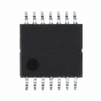
LX1744CPW Microsemi Analog Mixed Signal Group, LX1744CPW Datasheet - Page 3

LX1744CPW
Manufacturer Part Number
LX1744CPW
Description
IC LED DRVR WT/CLR BCKLT 14TSSOP
Manufacturer
Microsemi Analog Mixed Signal Group
Type
Backlight, White LED, Color LEDr
Datasheet
1.LX1744CPW.pdf
(16 pages)
Specifications of LX1744CPW
Constant Current
Yes
Topology
PWM, Step-Up (Boost)
Number Of Outputs
2
Internal Driver
Both
Type - Primary
Backlight
Type - Secondary
Color, White LED
Voltage - Supply
1.6 V ~ 6 V
Voltage - Output
25V
Mounting Type
Surface Mount
Package / Case
14-TSSOP
Operating Temperature
-40°C ~ 85°C
Current - Output / Channel
100mA
Internal Switch(s)
Yes
Efficiency
90%
Lead Free Status / RoHS Status
Lead free / RoHS Compliant
Frequency
-
Available stocks
Company
Part Number
Manufacturer
Quantity
Price
Company:
Part Number:
LX1744CPW
Manufacturer:
Microsemi Analog Mixed Signal
Quantity:
135
Copyright © 2000
Rev. 1.1b, 2005-03-01
SHDNx
LSHDN
Name
GND
DRV
SRC
OVP
BRT
REF
ADJ
LFB
SW
CS
FB
IN
I N T E G R A T E D
Unregulated IC Supply Voltage Input – Input range from +1.6V to 6.0V. Bypass with a 1µF or greater capacitor
for operation below 2.0V.
LED MOSFET Gate Driver – Connects to an external N-Channel MOSFET.
LED MOSFET Current Sense Input - Connects to the External N-Channel MOSFET Source.
Over Voltage Programming Pin – Connects to a resistor divider between the output load and GND to set the
maximum output voltage. OVP has a voltage threshold of 1.2V
LED Current Feedback Input – Connects to a current sense resistor between the LED output load and GND to
set the LED drive current.
Common terminal for ground reference.
LED Dimming Signal Input – Provides the internal reference, via an internal filter and gain resistor, allowing for a
dynamic output LED current adjustment that corresponds to the PWM input signal duty cycle. Either a PWM
signal or analog voltage can be used. The actual BRT pin voltage range is from V
current sense resistor power dissipation by selecting a range for V
Buffered Reference Output – Connected to the internal bandgap reference voltage of 1.2V.
LCD Bias Inductor Switch Connection – Internally connected to the drain of a 28V N-channel MOSFET. SW is
high impedance in shutdown.
Feedback Input – Connect to a resistive divider network between the output and GND to set the output voltage
between V
LCD Bias Adjustment PWM Signal Input – Connect to an RC filter allowing for dynamic output voltage adjustment
>±15%, corresponding to a varying duty cycle. Either a PWM signal or analog voltage can be used.
input voltage range is from 0.9V to V
reference is used.
LED Driver Active-Low Shutdown Input – A logic low shuts down the LED driver circuitry and reduces the supply
current by 60µA (Typ). Pull LSHDN high for normal operation.
LCD Bias Active-Low Shutdown Input – A logic low shuts down the LCD Bias circuitry and reduces the supply
current by 60µA (Typ). Pull SHDNx high for normal operation.
Current-Sense Amplifier Input – Connecting a resistor between CS and GND sets the peak inductor current limit.
11861 Western Avenue, Garden Grove, CA. 92841, 714-898-8121, Fax: 714-893-2570
CC
(IN) and 25V. The feedback threshold is 1.29V.
P R O D U C T S
F U N C T I O N A L P I N D E S C R I P T I O N
Integrated Products Division
IN
DC. The ADJx pin should be connected to ground when the internal
Microsemi
Dual Output Boost – LED Driver / LCD Bias
Description
P
RODUCTION
BRT
= 0.0V to 0.5V.
D
ATASHEET
IN
to GND. Minimize the
LX1744
The ADJ
Page 3


