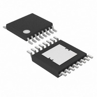
MAX16825AUE+ Maxim Integrated Products, MAX16825AUE+ Datasheet - Page 12

MAX16825AUE+
Manufacturer Part Number
MAX16825AUE+
Description
IC LED DRVR HIGH BRIGHT 16-TSSOP
Manufacturer
Maxim Integrated Products
Type
HBLED Driverr
Datasheet
1.MAX16824AUE.pdf
(13 pages)
Specifications of MAX16825AUE+
Constant Current
Yes
Topology
Linear, Open Drain, PWM
Number Of Outputs
3
Internal Driver
Yes
Type - Primary
Automotive, Backlight
Type - Secondary
High Brightness LED (HBLED)
Voltage - Supply
6.5 V ~ 28 V
Voltage - Output
36V
Mounting Type
Surface Mount
Package / Case
16-TSSOP Exposed Pad, 16-eTSSOP, 16-HTSSOP
Operating Temperature
-40°C ~ 125°C
Current - Output / Channel
150mA
Internal Switch(s)
Yes
Number Of Segments
6
Operating Supply Voltage
6.5 V to 28 V
Maximum Power Dissipation
1500 mW
Maximum Operating Temperature
+ 125 C
Mounting Style
SMD/SMT
Minimum Operating Temperature
- 40 C
Lead Free Status / RoHS Status
Lead free / RoHS Compliant
Frequency
-
Efficiency
-
Lead Free Status / Rohs Status
Details
A third method is to hold both LE and OE in the
enabled state. This allows the data bits to directly con-
trol the output channels, and hence, pulse dim the out-
put current. Make sure that the clock frequency does
not exceed the maximum rate at which the device can
change the state of the output channels.
The power dissipation (P
MAX16825 is determined from the following equation:
where:
V
V
I
High-Voltage, Three-Channel Linear
High-Brightness LED Drivers
PROCESS: BiCMOS-DMOS
12
P
IN
IN
INL
D
= supply current
= supply voltage
=
+
+
______________________________________________________________________________________
= supply voltage to the LED strings
(
(
(
V
V
V
IN
INL
INL
TOP VIEW
×
I
−
− V V
IN
V
) (
LED
LED
+
PWM1
PWM2
OUT1
N.C.
N.C.
CS1
REG
V
2
3
IN
INL
−
−
1
2
3
4
5
6
7
8
V
V
−
CS
CS
V
+
2
3
TSSOP-EP
LED
) (
) (
MAX16824
×
×
Chip Information
1
I
I
D
−
LED
LED
) of the MAX16824/
Power Dissipation
V
CS
2
3
1
×
×
) (
DUTY
DUTY
16
15
14
13
12
11
10
×
9
I
OUT2
CS2
N.C.
CS3
OUT3
GND
N.C.
PWM3
LED
2
3
1
)
)
×
DUT
Y Y
1
)
V
I
V
DUTY_ = PWM_ duty cycle
The worst-case power dissipation occurs when the
drop across each internal MOSFET is at its maximum
with all three channels delivering the maximum allow-
able output current. The maximum drop across the
internal MOSFETs is determined by:
Higher ambient temperature increases the thermal stress
even further due to the reduction in voltage drop across
the LEDs. The MAX16824/MAX16825 thermal specifica-
tions are given according to the JEDEC-51 guidelines.
Good mechanical/thermal design practices must be
applied to help maintain the device junction temperature
below the absolute maximum ratings at all times.
For the latest package outline information and land patterns, go
to www.maxim-ic.com/packages.
LED_
LED_
CS_
PACKAGE TYPE
V
16 TSSOP-EP
INL
= 200mV drop across R
= LED current
= total forward voltage for one LED string
- V
TOP VIEW
LED_
OUT1
- V
CS1
REG
N.C.
CLK
DIN
LE
IN
CS_
PACKAGE CODE
1
2
3
4
5
6
7
8
Package Information
when V
+
TSSOP-EP
U16E-3
MAX16825
Pin Configurations
CS_
LED_
is at its minimum.
16
15
14
13
12
11
10
9
DOCUMENT NO.
OUT2
CS2
N.C.
CS3
OUT3
GND
DOUT
OE
21-0108


