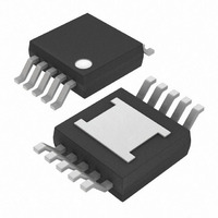
MAX7306AUB+ Maxim Integrated Products, MAX7306AUB+ Datasheet - Page 14

MAX7306AUB+
Manufacturer Part Number
MAX7306AUB+
Description
IC LED DRIVER LINEAR 10-UMAX
Manufacturer
Maxim Integrated Products
Type
Linear (I²C Interface)r
Datasheet
1.MAX7306AUB.pdf
(23 pages)
Specifications of MAX7306AUB+
Topology
PWM
Number Of Outputs
4
Internal Driver
Yes
Type - Primary
Backlight, LED Blinker
Type - Secondary
White LED
Frequency
1MHz
Voltage - Supply
1.62 V ~ 3.6 V
Mounting Type
Surface Mount
Package / Case
10-MSOP Exposed Pad, 10-HMSOP, 10-eMSOP
Operating Temperature
-40°C ~ 125°C
Current - Output / Channel
25mA
Internal Switch(s)
No
Lead Free Status / RoHS Status
Lead free / RoHS Compliant
Voltage - Output
-
Efficiency
-
Lead Free Status / Rohs Status
Details
SMBus/I
GPIOs and LED Drivers
the host processor of data changes at the selected
inputs. Reset INT by reading any port’s I/O registers
(0x01 to 0x04).
Upon power-up, the MAX7306/MAX7307 enter standby
mode when the serial interface is idle. If any of the PWM
intensity control, blink, or debounce features are used,
the operating current rises because the internal PWM
oscillator is running and toggling counters. When using
OSCIN to override the internal oscillator, the operating
current varies according to the frequency at OSCIN.
When the serial interface is active, the operating current
also increases because the MAX7306/MAX7307, like all
I
timeout circuit and debounce circuit use the internal oscil-
lator even if OSCIN is selected.
The MAX7306/MAX7307 contain an internal oscillator
nominally at 32kHz. The MAX7306/MAX7307 always use
the internal oscillator for bus timeout and for debounce
timing (when enabled). The internal oscillator is also
used by default to generate PWM and blink timing. The
internal oscillator only runs when the clock output
OSCOUT is needed to keep the operating current as
low as possible.
The MAX7306/MAX7307 can use an external clock
source instead of the internal oscillator for the PWM
and blink timing. The external clock can range from DC
to 1MHz and it connects to the P2/OSCIN port. The
P3/OSCOUT port provides a buffered and level-shifted
output of the internal oscillator or external clock to drive
other devices. Select the P2/OSCIN and P3/OSCOUT
Figure 4. Synchronizing Multiple MAX7306/MAX7307s (Internal Oscillator)
14
2
C slaves, have to monitor every transmission. The bus
______________________________________________________________________________________
Internal Oscillator and OSCIN/OSCOUT
2
C Interfaced 4-Port, Level-Translating
MAX7306/MAX7307
MAX7306/MAX7307
External Clock Options
P3/OSCOUT
P3/OSCOUT
Standby Mode
P2/OSCIN
P2/OSCIN
MAX7306/MAX7307
MAX7306/MAX7307
port options using the device configuration register
0x27 bits D2 and D3 (see Table 2).
The P2/OSCIN port is overvoltage protected to supply
voltage V
exceed V
clock cannot exceed V
register (see Tables 2 and 6) sets the P2/OSCIN logic
threshold (30%/70%) to either the V
Use OSCOUT or an external clock source to cascade
up to four MAX7306s per master for applications requir-
ing additional ports. To synchronize the blink action
across multiple MAX7306s (see Figures 4 and 5), use
OSCOUT from one MAX7306 to drive OSCIN of the
other MAX7306s. This process ensures the same blink
frequency of all the devices, but also make sure to syn-
chronize the blink phase. The blink timing of multiple
MAX7306s is synchronous at the instant of power-up
because the blink and PWM counters clear by each
device’s internal reset circuit, and by default the
device’s internal oscillators are off upon power-up.
Ensure that the blink phase of all the devices remains
synchronized by programming the OSCIN and
OSCOUT functionality before programming any feature
that causes a MAX7306’s internal oscillator to operate
(blink, PWM, bus timeout, or key debounce). Configure
the RST input to reset the internal timing counters used
for PWM and blink by setting bit D1 of device configu-
ration register 0x26 (see Table 3).
P3/OSCOUT
LA
DD
for the MAX7307, so the external clock can
if V
P2/OSCIN
P2/OSCIN
LA
MAX7306/MAX7307
MAX7306/MAX7307
is greater than V
DD
for the MAX7306. The port P2
DD
supply or the V
DD
. The external
LA
.


