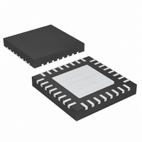
MAX16816ATJ+ Maxim Integrated Products, MAX16816ATJ+ Datasheet - Page 12

MAX16816ATJ+
Manufacturer Part Number
MAX16816ATJ+
Description
IC LED DRIVR HIGH BRIGHT 32-TQFN
Manufacturer
Maxim Integrated Products
Type
HBLED Driverr
Datasheet
1.MAX16816ATJ.pdf
(33 pages)
Specifications of MAX16816ATJ+
Topology
PWM, SEPIC, Step-Down (Buck), Step-Up (Boost)
Number Of Outputs
1
Internal Driver
Yes
Type - Primary
Automotive
Type - Secondary
High Brightness LED (HBLED)
Frequency
125kHz ~ 500kHz
Voltage - Supply
5.5 V ~ 76 V
Mounting Type
Surface Mount
Package / Case
32-TQFN Exposed Pad
Operating Temperature
-40°C ~ 125°C
Internal Switch(s)
Yes
Efficiency
90%
Low Level Output Current
76 mA
High Level Output Current
67 mA
Operating Supply Voltage
5.5 V to 76 V
Maximum Supply Current
4.5 mA
Maximum Power Dissipation
2758 mW
Maximum Operating Temperature
+ 125 C
Mounting Style
SMD/SMT
Minimum Operating Temperature
- 40 C
Lead Free Status / RoHS Status
Lead free / RoHS Compliant
Voltage - Output
-
Current - Output / Channel
-
Lead Free Status / Rohs Status
Details
Programmable Switch-Mode LED Driver
with Analog-Controlled PWM Dimming
12
9, 10, 11
16, 17
1, 24
PIN
12
13
14
15
18
19
20
2
3
4
5
6
7
8
______________________________________________________________________________________
CLKOUT
RTSYNC
NAME
AGND
COMP
SGND
UVEN
REG1
SNS+
N.C.
DRV
REF
DIM
DRI
I.C.
CS
OV
FB
No Connection. Not internally connected.
Undervoltage Lockout (UVLO) Threshold/Enable Input. UVEN is a dual-function adjustable UVLO threshold
input with an enable feature. Connect UVEN to V
threshold. Connect UVEN directly to V
greater than 1.244V to UVEN to enable the device.
5V Regulator Output. REG1 is an internal low-dropout voltage regulator that generates a 5V (V
output voltage and supplies power to internal circuitry. Bypass REG1 to AGND through a 1µF ceramic
capacitor.
Analog Ground. Use proper single-point ground design and decoupling to avoid ground impedance loop
errors.
Accurate 3V Buffered Reference Output. Connect REF to DIM through a resistive voltage-divider to apply a
DC voltage for analog-controlled dimming functionality. Leave REF unconnected if unused.
Dimming Control Input. Connect DIM to an external PWM signal for PWM dimming. For analog-controlled
dimming, connect DIM to REF through a resistive voltage-divider. The dimming frequency is 200Hz under
these conditions. Connect DIM to AGND to turn off the LEDs.
Sync Input/Output. The internal PWM clock is selectable through the RTOF EEPROM bit. Connect an
external resistor to RTSYNC and set the RTOF register to ‘0’ to select a clock frequency between 125kHz
and 500kHz. Set RTOF register to ‘0’ and connect RTSYNC to an external clock to synchronize the device
with external clock. Set RTOF register to ‘1’ to use the fixed 125kHz oscillator. Under these conditions,
RTSYNC is powered off and may be left in any state. See the Oscillator, Clock, and Synchronization section.
Clock Output. CLKOUT buffers the oscillator/clock. Connect CLKOUT to the SYNC input of another device
to operate the MAX16816 in a multichannel configuration. CLKOUT is a logic output.
Internally Connected. Must be connected to AGND.
Error-Amplifier Output. Connect the compensation network from COMP to FB for stable closed-loop control.
Use low-leakage ceramic capacitors in the feedback network.
Current-Sense Voltage Output. CS outputs a voltage proportional to the current sensed through the current-
sense amplifier. Connect CS through a passive network to FB as dictated by the chosen compensation
scheme.
Error-Amplifier Inverting Input
Overvoltage Protection Input. Connect OV to HI through a resistive voltage-divider to set the overvoltage
limit for the load. When the voltage at OV exceeds the 1.235V (typ) threshold, an overvoltage fault is
generated and the switching MOSFET turns off. The MOSFET is turned on again when the voltage at OV
drops below 1.17V (typ).
Gate-Driver Output. Connect DRV through a series resistor to the gate of an external n-channel MOSFET to
reduce EMI. DRV can sink 1A or source 0.5A.
Gate-Driver Supply Input. Connect DRI to REG2 to power the primary switching MOSFET driver.
Positive Peak Current-Sense Input. Connect SNS+ to the positive side of the switch current-sense resistor,
R
Switching Ground. SGND is the ground for non-analog and high-current gate-driver circuitry.
SENSE
.
CC
to use the 5.9V (max) default UVLO threshold. Apply a voltage
CC
FUNCTION
through a resistive voltage-divider to program the UVLO
Pin Description
CC
> 6V)


