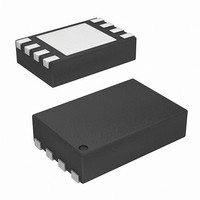
ISL97632IRT18Z-T Intersil, ISL97632IRT18Z-T Datasheet - Page 8

ISL97632IRT18Z-T
Manufacturer Part Number
ISL97632IRT18Z-T
Description
IC LED DRIVR WHITE BCKLGT 8-TDFN
Manufacturer
Intersil
Type
Backlight, White LEDr
Datasheet
1.ISL97632IRT26Z-TK.pdf
(9 pages)
Specifications of ISL97632IRT18Z-T
Topology
PWM, Step-Up (Boost)
Number Of Outputs
1
Internal Driver
Yes
Type - Primary
Automotive, Backlight
Type - Secondary
White LED
Frequency
1.3MHz ~ 1.6MHz
Voltage - Supply
2.4 V ~ 5.5 V
Mounting Type
Surface Mount
Package / Case
8-TDFN Exposed Pad
Operating Temperature
-40°C ~ 85°C
Current - Output / Channel
50mA
Internal Switch(s)
Yes
Efficiency
86%
Lead Free Status / RoHS Status
Lead free / RoHS Compliant
Voltage - Output
-
SEPIC Operation
For applications where the output voltage is not always
above the input voltage, a buck or boost regulation is
needed. A SEPIC (Single Ended Primary Inductance
Converter) topology, (see Figure 10), can be considered for
such an application. A single cell Li-Ion battery operating a
cellphone backlight or flashlight is one example. The
battery voltage is between 2.5V and 4.2V depending on the
state of charge. On the other hand, the output may require
only one 3V to 4V medium power LED for illumination
because the light guard of the backlight assembly is
optimized or it is a cost efficiency trade off reason.
In fact, a SEPIC configured LED driver is flexible enough to
allow the output to be well above or below the input voltage,
unlike the previous example. Another example is when the
number of LEDs and input requirements are different from
platform to platform, a common circuit and PCB that fit all the
platforms, in some cases, may be beneficial enough that it
outweighs the disadvantage of adding additional component
cost. L1 and L2 can be a coupled inductor in one package.
The simplest way to understand SEPIC topology is to think
about it as a boost regulator in which the input volute is level
shifted downward at the same magnitude and the lowest
reference level starts at -V
The SEPIC works as follows: Assume the circuit in Figure 10
operates normally when the ISL97632 internal switch opens,
and it is in the PWM ‘OFF’ state. After a short duration where
few LC time constants elapsed, the circuit is considered in
the steady-state within the PWM ‘OFF’ period that L1 and L2
are shorted. V
charged to V
switch closes, and the circuit is in the PWM on state, V
now pulled to ground. Since the voltage in C3 cannot be
changed instantaneously, V
becomes -V
opens, V
boost regulator operation, except the lowest reference point
is at -V
Equation 5:
V
VIN = 2.7V to 5.5V
OUT
1µF
C1
0.1µF
=
C2
IN
B
. The output is approximated as shown in
V
IN
boosts up to the targeted output like the standard
IN
----------------- -
(
IN
1 D
. The next cycle, when the ISL97632 switch
B
FIGURE 10. SEPIC LED DRIVER
D
–
with V
is therefore shorted to the ground and C3 is
VIN
EN
SDIN
1
)
22µH
L1
A
FBSW
VOUT
= V
2
GND
FB
LX
IN
IN
B
rather than 0V.
. When the ISL97632 internal
is shifted downward and
8
V
A
1µF
R1
C3
1Ω
V
B
22µH
L2
C4 0.22µ
(EQ. 5)
A
D1
is
ISL97632
where D is the on-time of the PWM duty cycle.
The convenience of SEPIC comes with some trade off in
addition to the additional L and C costs. The efficiency is
usually lowered because of the relatively large efficiency
loss through the Schottky diode if the output voltage is low.
The L2 series resistance also contributes additional loss.
Figure 11 shows the efficiency measurement of a single LED
application as the input varies between 2.7V and 4.2V.
Note, V
standard boost regulator. The higher the input voltage, the
lower the V
result is that the efficiency will be lower at higher input
voltages because the SEPIC has to work harder to boost up
to the required level. This behavior is the opposite to the
standard boost regulator’s and the comparison is shown in
Figure 11.
PCB Layout Considerations
The layout is very important for the converter to function
properly. R
and GND pins. Longer traces to the LEDs are acceptable.
Similarly, the supply decoupling capacitor and the output filter
capacitor should be as close as possible to the VIN and
VOUTpins.
The heat of the IC is mainly dissipated through the thermal
pad of the package. Maximize the copper area connected to
this pad if possible. In addition, a solid ground plane is always
helpful for the EMI performance.
FIGURE 11. EFFICIENCY MEASUREMENT OF 1 LED SEPIC
76
72
68
64
60
B
0
is considered the level-shifted LX node of a
SET
B
voltage will be during PWM on period. The
DRIVER
must be located as close as possible to the FB
5
ILED (mA)
V
V
IN
IN
10
= 4.2V
= 2.7V
1 LED
L1 = L2 = 22µH
C3 = 1µF
R1 = 4.7Ω
15
March 22, 2010
FN9239.3
20


