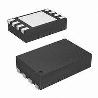
ISL97634IRT14Z-T Intersil, ISL97634IRT14Z-T Datasheet - Page 8

ISL97634IRT14Z-T
Manufacturer Part Number
ISL97634IRT14Z-T
Description
IC LED DRIVR WHITE BCKLGT 8-TDFN
Manufacturer
Intersil
Type
Backlight, White LEDr
Datasheet
1.ISL97634IRT14Z-T.pdf
(10 pages)
Specifications of ISL97634IRT14Z-T
Topology
PWM, Step-Up (Boost)
Number Of Outputs
1
Internal Driver
Yes
Type - Primary
Automotive, Backlight
Type - Secondary
White LED
Frequency
1.3MHz ~ 1.6MHz
Voltage - Supply
2.4 V ~ 5.5 V
Mounting Type
Surface Mount
Package / Case
8-TDFN Exposed Pad
Operating Temperature
-40°C ~ 85°C
Current - Output / Channel
70mA
Internal Switch(s)
Yes
Efficiency
85%
Lead Free Status / RoHS Status
Lead free / RoHS Compliant
Voltage - Output
-
Available stocks
Company
Part Number
Manufacturer
Quantity
Price
Company:
Part Number:
ISL97634IRT14Z-TK
Manufacturer:
Intersil
Quantity:
3 000
V
These equations are valid for values of R
both R
The analog dimming circuit can be tailored to a desired
relative brightness for different V
Equation 8.
R
Where V
the minimum relative brightness (i.e., the brightness with
V
i.e., V
i.e., V
Efficiency Improvement
Figure 1 shows the efficiency measurements during PWM
operation. The choice of the inductor has a significant impact
on the power efficiency. As shown in Equation 4, the higher
the inductance, the lower the peak current, therefore, the
lower the conduction and switching losses. On the other hand,
it has also a higher series resistance. Nevertheless, the
efficiency improvement effect by lowering the peak current is
greater than the resistance increases with larger value of
inductor. Efficiency can also be improved for systems that
have high supply voltages. Since the ISL97634 can only
supply from 2.4V to 5.5V, V
high supply voltage for the boost circuit as shown in Figure 15
and the efficiency improvement is shown in Figure 16.
IN
Vs = 12V
2
Dim_max
= 2.7V TO 5.5V
FIGURE 15. SEPARATE HIGH INPUT VOLTAGE FOR HIGHER
C1
=
C2
[
-------------------------------------------------------------------
Dim_max
Dim_max
(
1
V
1µF
>>RSET and R
0.1µF
Dim_max
[
Dim_max
V
applied).
FB
EFFICIENCY OPERATION
•
= 5V, F
= 1V, F
1
VIN
PWM/EN
(
1 F
–
ISL97634
–
is the maximum V
22µH
V
L1
FB
min
min
min
FBSW
) R
VOUT
2
•
)
GND
>>RSET.
]
2
FB
LX
= 10% (i.e., 0.1), R
= 10% (i.e., 0.1), R
1
IN
]
must be separated from the
8
Dim
Dim
ranges using
voltage and F
1
C3 0.22µF
and R
2
2
R1
= 189k
= 35k
2
such that
4Ω
D1
D2
D3
D4
D5
D6
(EQ. 8)
min
is
ISL97634
.
8 LEDs Operation
For medium size LCDs that need more than 7 low power LEDs
for backlighting, such as a portable media player or automotive
navigation panel displays, the voltage range of the ISL97634 is
not sufficient. However, the ISL97634 can be used as an LED
controller with an external protection MOSFET connected in
cascode fashion to achieve higher output voltage. A conceptual
8 LEDs driver circuit is shown in Figure 17. A 60V logic level N-
Channel MOSFET is configured such that its drain ties between
the inductor and the anode of Schottky diode, its gate ties to the
input, and its source ties to the ISL97634 LX node connecting
to the drain of the internal switch. When the internal switch
turns on, it pulls the source of M1 down to ground and LX
conducts as normal. When the internal switch turns off, the
source of M1 will be pulled up by the follower action of M1,
limiting the maximum voltage on the ISL97634 LX pin to below
V
breakdown limit on the LX pin. The switch current limit and
maximum duty cycle will not be changed by this setup, so input
voltage will need to be carefully considered to make sure that
the required output voltage and current levels are achievable.
Because the source of M1 is effectively floating when the
internal LX switch is off, the drain-to-source capacitance of M1
may be sufficient to capacitively pull the node high enough to
break down the gate oxide of M1. To prevent this, V
be connected to V
limit the peak voltage. This will also hold the VOUT pin at a
known low voltage, preventing the built in OVP function from
causing problems. This OVP function is effectively useless in
this mode as the real output voltage is outside its intended
range. If the user wants to implement their own OVP protection
(to prevent damage to the output capacitor), they should insert
a zener diode from VOUT to the FB pin. In this setup, it would
be wise not to use the FBSW to FB switch, as otherwise, the
zener diode will have to be a high power one capable of
dissipating the entire LED load power. Then the LED stack can
then be connected directly to the sense resistor via a 10kΩ
resistor to FB. A zener can be placed from VOUT to the FB pin
allowing an overvoltage event to pull-up on FB with a low
breakdown current (and thus low power zener diode) as a
result of the 10kΩ resistor.
IN
FIGURE 16. EFFICIENCY IMPROVEMENT WITH 9 AND 12V
, but allowing the output voltage to go much higher than the
90
85
80
75
70
0
INPUTS
5
IN
V
, allowing the internal Schottky diode to
S
= 12V
10
ILED (mA)
15
20
V
S
= 9V
V
7 LEDs
L1 = 22µH
R1 = 4Ω
f
PWM
IN
25
OUT
= 4V
March 7, 2008
should
FN6264.3
30


