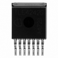
TLE4242G Infineon Technologies, TLE4242G Datasheet - Page 2

TLE4242G
Manufacturer Part Number
TLE4242G
Description
IC LED DRIVER LINEAR D2PAK
Manufacturer
Infineon Technologies
Type
Linear (Non-Switching)r
Datasheet
1.TLE4242G.pdf
(14 pages)
Specifications of TLE4242G
Package / Case
D²Pak, TO-263 (7 leads + tab)
Constant Current
Yes
Topology
Linear (LDO), PWM
Number Of Outputs
1
Internal Driver
Yes
Type - Primary
Automotive, General Purpose
Voltage - Supply
4.5 V ~ 42 V
Voltage - Output
40V
Mounting Type
Surface Mount
Operating Temperature
-40°C ~ 150°C
Current - Output / Channel
500mA
Internal Switch(s)
Yes
Number Of Segments
3
Operating Supply Voltage
4.5 V to 42 V
Maximum Operating Temperature
+ 150 C
Mounting Style
SMD/SMT
Minimum Operating Temperature
- 40 C
Lead Free Status / RoHS Status
Lead free / RoHS Compliant
For Use With
DEMOBOARDTLE4242GIN - BOARD DEMO FOR TLE4242G
Frequency
-
Efficiency
-
Lead Free Status / Rohs Status
Details
Other names
SP000014456
SP000299340
TLE4242GINTR
TLE4242GNT
TLE4242GT
TLE4242GT
TLE4242GXT
SP000299340
TLE4242GINTR
TLE4242GNT
TLE4242GT
TLE4242GT
TLE4242GXT
Available stocks
Company
Part Number
Manufacturer
Quantity
Price
Company:
Part Number:
TLE4242GATMA3
Manufacturer:
INFINEON
Quantity:
12 000
Circuit Description
Figure 1
An external shunt resistor in the ground path of the connected LEDs is used to sense the
LED current. A regulation loop helds the voltage drop at the shunt resistor on a constant
level of typ. 177 mV. Selecting the shunt resistance permits to adjust the appropriate
constant current level. The typ. output current calculates
where
equation applies in a range of 0.39 Ω ≤
The output current is shown as a function of the reference resistance on
the PWM input the LED brightness can be regulated via duty cycle. Also PWM = L sets
the TLE 4242 in sleep mode resulting in a very low current consumption of << 1 μA typ.
Due to the high impedance of the PWM input (see
PWM Voltage” on Page
Data Sheet
I
Q typ
,
PWM
=
V
REF
V
------------
R
I
REF
REF
1
2
is the reference voltage with a typical level of 177 mV (see
Block Diagram
Bias Supply
Reference
Bandgap
11) the PWM pin can thus also be used as an enable input.
R
GND
REF
4
2
≤ 1.8 Ω.
Comparator
Status
Delay
D
6
“PWM Pin Input Current versus
AEB03500.VSD
Rev. 1.1, 2007-03-20
Page
Page
TLE 4242 G
7
5
3
Q
REF
ST
10). The
10. With
(1)


