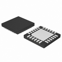
NCP5680MUTXG ON Semiconductor, NCP5680MUTXG Datasheet - Page 16

NCP5680MUTXG
Manufacturer Part Number
NCP5680MUTXG
Description
IC LED DRIVER WHT HI EFF 24-UQFN
Manufacturer
ON Semiconductor
Type
Photo Flash LED (I²C Interface)r
Datasheet
1.NCP5680MUTXG.pdf
(27 pages)
Specifications of NCP5680MUTXG
Topology
Switched Capacitor (Charge Pump)
Number Of Outputs
2
Internal Driver
No
Type - Primary
Flash/Torch
Type - Secondary
White LED
Frequency
850kHz ~ 1.15MHz
Voltage - Supply
2.7 V ~ 5.5 V
Voltage - Output
4.5 V ~ 5.3 V
Mounting Type
Surface Mount
Package / Case
24-UFQFN Exposed Pad, 24-UFQFN
Operating Temperature
-40°C ~ 85°C
Current - Output / Channel
400mA
Internal Switch(s)
Yes
Lead Free Status / RoHS Status
Lead free / RoHS Compliant
Efficiency
-
Lead Free Status / Rohs Status
Details
Available stocks
Company
Part Number
Manufacturer
Quantity
Price
Company:
Part Number:
NCP5680MUTXG
Manufacturer:
ON Semiconductor
Quantity:
2 050
Load Connection
two high power LED arranged in the photo flash structure.
The LED are independently activated or de−activated by
means of the I2C command.
or the Indicator function, the output LED current being
monitored by the associated current mirrors. Although it is
possible to connect several LED in parallel to share the
output current, such solution is discouraged since the
matching between the LED can no longer be guaranteed.
package provides a way to drive up to four LEDs with full
flash current capability per LED, as depicted in Figure 11.
LED Programming Operation
of an hexadecimal byte coming from the I2C port. The Iout
peak current, the flash pulse duration and the flash delays
are stored into registers associated to each LED.
Consequently, each LED can have a different amplitude,
duration and delay during a single photo flash sequence.
Picture Light or ICON − is selected by the I2C command.
In addition, the photo flash sequence can be activated either
by the appropriate I2C command, or by means of the
dedicated TRGFL pin, assuming the chip has been
previously activated (the TRGFL signal has no effect if
NCP5680 is in shut down mode). The Time out is
automatically asserted when a pulsed flash is activated.
Power Flash
analog loop built with the external NMOS device
The primary function of the NCP5680 chip is to control
In addition, the chip is capable to drive the Torch mode
However, using a dual NMOS device in the same
All the electrical biases of each LED are set up by means
The mode of operation − either Video torch or Flash, or
The I−LED flash current is regulated by means of the
TRIGFL
FLASH
PHOTO SENSE
Mode
PHOTO SENSE
Feedback
Charge Pump
Active
Standby
T
FW
≥ 10 ms
Photo sense function activated
Illumination level is preset by
the I2C previous message
Cout = 1F, Vbat = 4V
Figure 11. Basic Operation Timings
Re−cycle: 2sec @
http://onsemi.com
16
Photo sense feedback
associated to the external shunt resistor: see Figure 10. The
internal operational amplifier uses the reference voltages,
as defined by the contain of register FILED1 and FILED2,
to monitor the current flowing in the loop. Basically, the
Voltage to current ratio is 100 mV/A: a 100 mW resistor will
force a 1 A I−LED current with 100 mV programmed at the
FILED1 or FILED2 register. Of course, different value for
the shunt resistor can be implemented, but care must be
observed as it might be difficult to extract a low drop
voltage in a noisy environment.
The power flash sequence can be activated in two ways:
1. Using the I2C command associated to the
2. Using a direct command through the TRGFL pin,
CONFIG1register: the positive going of the bit
I2CTRG signal fires the pulsed flash (the pulse
width depends upon the contain of FLWID1 &
FLWID2 registers), the delays are activated,
depending upon the contain of FLDY1 & FLDY2
registers, the time out is engaged, the output
current is forced to the values previously stored
into the FILED1 and FILED2 registers. The flash
can be as short as 100 ms, with 255 ms as a
maximum duration (see TOUT register). The
I2CTRG bit in the CONFIG1 register is
automatically reset to Low when the flash pulse
is completed.
assuming the EXTRG bit in the CONFIG1
register is set to High. In this case, the time out is
activated but the timers and the pulse width
registers are de−activated since the duration of
the pulsed flash depends solely upon the duration
of the signal present at the TRGFL pin.
T
FW
TRIGFL Pulse


