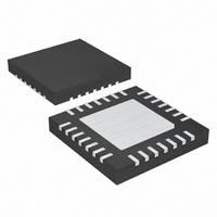
MAX16821AATI+ Maxim Integrated Products, MAX16821AATI+ Datasheet - Page 18

MAX16821AATI+
Manufacturer Part Number
MAX16821AATI+
Description
IC LED DRIVR HIGH BRIGHT 28-TQFN
Manufacturer
Maxim Integrated Products
Type
HBLED Driverr
Datasheet
1.MAX16821BATI.pdf
(24 pages)
Specifications of MAX16821AATI+
Topology
High Side, Low Side, PWM, SEPIC, Step-Down (Buck), Step-Up (Boost)
Number Of Outputs
1
Internal Driver
No
Type - Primary
Automotive, Backlight
Type - Secondary
High Brightness LED (HBLED)
Frequency
125kHz ~ 1.5MHz
Voltage - Supply
4.75 V ~ 5.5 V, 7 V ~ 28 V
Voltage - Output
5.1V
Mounting Type
Surface Mount
Package / Case
28-TQFN Exposed Pad
Operating Temperature
-40°C ~ 125°C
Current - Output / Channel
30A
Internal Switch(s)
Yes
Low Level Output Current
4000000 uA (Typ)
High Level Output Current
4000000 uA (Typ)
Operating Supply Voltage
7 V to 28 V
Maximum Supply Current
5.5 mA
Maximum Power Dissipation
2758 mW
Maximum Operating Temperature
+ 125 C
Mounting Style
SMD/SMT
Minimum Operating Temperature
- 40 C
Lead Free Status / RoHS Status
Lead free / RoHS Compliant
Efficiency
-
Lead Free Status / Rohs Status
Lead free / RoHS Compliant
The switching frequency, peak inductor current, and
allowable ripple at the output determine the value and
size of the inductor. Selecting higher switching frequen-
cies reduces inductance requirements, but at the cost
of efficiency. The charge/discharge cycle of the gate
and drain capacitance in the switching MOSFETs cre-
ate switching losses worsening at higher input volt-
ages, since switching losses are proportional to the
square of the input voltage. The MAX16821A/
MAX16821B/MAX16821C operate up to 1.5MHz.
Choose inductors from the standard high-current, sur-
face-mount inductor series available from various manu-
facturers. Particular applications may require
custom-made inductors. Use high-frequency core mate-
rial for custom inductors. High ΔI
peak flux excursion increasing the core losses at higher
frequencies. The high-frequency operation coupled with
high ΔI
makes the use of planar inductors possible.
The following discussion is for buck or continuous
boost-mode topologies. Discontinuous boost, buck-
boost, and SEPIC topologies are quite different in
regards to component selection. Use the following
equations to determine the minimum inductance value:
Buck regulators:
Boost regulators:
where V
The average current-mode control feature of the
MAX16821A/MAX16821B/MAX16821C limits the maxi-
mum peak inductor current and prevents the inductor
from saturating. Choose an inductor with a saturating
current greater than the worst-case peak inductor cur-
rent. Use the following equation to determine the worst-
case current in the average current-mode control loop.
where R
the buck converter, the sense current is the inductor
current and for the boost converter, the sense current is
the input current.
High-Power Synchronous HBLED
Drivers with Rapid Current Pulsing
18
______________________________________________________________________________________
L
L
LED
S
reduces the required minimum inductance and
MIN
L
is the sense resistor and V
MIN
is the total voltage across the LED string.
I
=
LPEAK
=
(
V
(
LED
V
INMAX
V
V
INMAX
=
LED
−
V
R
CL
V
S
INMAX
−
×
×
+
V
f
SW
Inductor Selection
LED
f
L
SW
⎛
⎜
⎝
causes large peak-to-
)
Δ
× Δ
I
)
×
2
CL
× Δ
×
CL
V
⎞
⎟
⎠
I
INMAX
L
V
I
LED
L
= 0.030V. For
When choosing a MOSFET for voltage regulators, con-
sider the total gate charge, R
and package thermal impedance. The product of the
MOSFET gate charge and on-resistance is a figure of
merit, with a lower number signifying better perfor-
mance. Choose MOSFETs optimized for high-frequen-
cy switching applications. The average current from the
MAX16821A/MAX16821B/MAX16821C gate-drive out-
put is proportional to the total capacitance it drives
from DH and DL. The power dissipated in the
MAX16821A/MAX16821B/MAX16821C is proportional
to the input voltage and the average drive current. The
gate charge and drain capacitance losses (CV
cross-conduction loss in the upper MOSFET due to
finite rise/fall time, and the I
in the MOSFET R
the MOSFET. Estimate the power loss (PD
high-side and low-side MOSFETs using the following
equations:
where Q
MOSFET’s total gate charge, on-resistance, rise time,
and fall time, respectively.
For the buck regulator, D is the duty cycle, I
(I
The discontinuous input-current waveform of the buck
converter causes large ripple currents in the input
capacitor. The switching frequency, peak inductor cur-
rent, and the allowable peak-to-peak voltage ripple
reflected back to the source dictate the capacitance
requirement. The input ripple is comprised of ΔV
(caused by the capacitor discharge) and ΔV
(caused by the ESR of the capacitor).
I
OUT
RMS HI
PD
I
RMS LO
MOS LO
PD
−
−
- ΔI
MOS HI
_
G
L
=
, R
=
/ 2) and I
_
=
DS(ON
⎛
⎝
(
I
I
2
(
2
Q
VALLEY
VALLEY
=
G
DS(ON)
(
R
⎡
⎢
⎢
⎣
), t
Q
×
V
PK
DS ON
G
IN
V
R
DD
(
+
= (I
, and t
×
×
+
I
2
account for the total losses in
×
)
V
PK
I
I
LED
OUT
2
DD
×
PK
f
2
SW
R loss due to RMS current
+
DS(ON)
Switching MOSFETs
F
I
2
×
)
+ ΔI
×
I
RMS HI
+
are the upper-switching
VALLEY
+
2
f
(
SW
I
t
Input Capacitors
VALLEY
R
R
L
−
DS ON
, power dissipation,
+
)
/ 2).
t
(
+
F
×
)
I
)
PK
×
×
×
MOS_
)
f
I
SW
I
PK
2
×
RMS LO
VALLEY
(
⎞
⎠ ×
⎤
⎥
⎥
⎦
1
) in the
−
2
3
−
+
D
), the
)
ESR
D
3
Q
=


