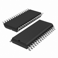
PCA9625D/S911,518 NXP Semiconductors, PCA9625D/S911,518 Datasheet - Page 7

PCA9625D/S911,518
Manufacturer Part Number
PCA9625D/S911,518
Description
IC LED DRIVER RGBA 32-SOIC
Manufacturer
NXP Semiconductors
Type
RGBA LED Driverr
Datasheet
1.PCA9625D512.pdf
(33 pages)
Specifications of PCA9625D/S911,518
Topology
Open Drain, PWM
Number Of Outputs
16
Internal Driver
Yes
Type - Primary
Backlight, LED Blinker
Type - Secondary
RGBA
Frequency
1MHz
Voltage - Supply
2.3 V ~ 5.5 V
Voltage - Output
24V
Mounting Type
Surface Mount
Package / Case
32-SOIC (7.5mm Width)
Operating Temperature
-40°C ~ 85°C
Current - Output / Channel
100mA
Internal Switch(s)
Yes
Lead Free Status / RoHS Status
Lead free / RoHS Compliant
Efficiency
-
Other names
935285147518
PCA9625D/S911-T
PCA9625D/S911-T
PCA9625D/S911-T
PCA9625D/S911-T
NXP Semiconductors
PCA9625_2
Product data sheet
7.1.2 LED All Call I
7.1.3 LED Sub Call I
7.1.4 Software Reset I
The last bit of the address byte defines the operation to be performed. When set to logic 1
a read is selected, while a logic 0 selects a write operation.
See
Remark: The default LED All Call I
as a regular I
PCA9625s on the I
See
Remark: The default LED Sub Call I
slave addresses as long as they are disabled.
The address shown in
performed by the master. The Software Reset address (SWRST Call) must be used with
R/W = logic 0. If R/W = logic 1, the PCA9625 does not acknowledge the SWRST. See
Section 7.6 “Software Reset”
Fig 3.
•
•
•
•
•
•
•
Default power-up value (ALLCALLADR register): E0h or 1110 000
Programmable through I
At power-up, LED All Call I
E0h (R/W = 0) or E1h (R/W = 1) is sent by the master.
3 different I
Default power-up values:
– SUBADR1 register: E2h or 1110 001
– SUBADR2 register: E4h or 1110 010
– SUBADR3 register: E8h or 1110 100
Programmable through I
At power-up, Sub Call I
ACK when E2h (R/W = 0) or E3h (R/W = 1), E4h (R/W = 0) or E5h (R/W = 1), or
E8h (R/W = 0) or E9h (R/W = 1) is sent by the master.
Section 7.3.8 “ALLCALLADR, LED All Call I
Section 7.3.7 “SUBADR1 to SUBADR3, I
Slave address
2
C-bus slave address since this address is enabled at power-up. All the
2
2
C-bus addresses can be used
C-bus address
2
C-bus addresses
2
2
C-bus will acknowledge the address if sent by the I
C-bus address
Rev. 02 — 15 January 2008
Figure 4
2
C-bus addresses are disabled. PCA9625 does not send an
2
2
C-bus (volatile programming)
C-bus (volatile programming)
for more detail.
A6
2
C-bus address is enabled. PCA9625 sends an ACK when
is used when a reset of the PCA9625 needs to be
A5
2
hardware selectable
C-bus address (E0h or 1110 000) must not be used
2
C-bus addresses may be used as regular I
slave address
A4
A3
16-bit Fm+ I
A2
2
C-bus subaddress 1 to 3”
2
C-bus address”
A1
002aab319
A0
2
R/W
C-bus 100 mA 24 V LED driver
for more detail.
PCA9625
2
© NXP B.V. 2008. All rights reserved.
C-bus master.
for more detail.
2
C-bus
7 of 33


