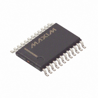
DS3881E+C Maxim Integrated Products, DS3881E+C Datasheet - Page 26

DS3881E+C
Manufacturer Part Number
DS3881E+C
Description
IC CCFL CONTROL 24TSSOP
Manufacturer
Maxim Integrated Products
Type
CCFL Controllerr
Datasheet
1.DS3881EC.pdf
(28 pages)
Specifications of DS3881E+C
Frequency
40 ~ 100 kHz
Current - Supply
12mA
Voltage - Supply
4.75 V ~ 5.25 V
Operating Temperature
-40°C ~ 105°C
Package / Case
24-TSSOP
Operating Supply Voltage
5 V
Maximum Operating Temperature
- 40 C
Mounting Style
SMD/SMT
Minimum Operating Temperature
+ 105 C
Supply Current
12 mA
Lead Free Status / RoHS Status
Lead free / RoHS Compliant
Current - Output
-
Lead Free Status / Rohs Status
Lead free / RoHS Compliant
Other names
DS3881E+
DS3881E+
DS3881E+
Each DS3881 responds to one of four possible slave
addresses based on the state of the address input pins
(A0 and A1). For information about device addressing,
see the I
Resistor R7 and R8 in the Typical Operating Circuit set
the lamp current. R7 and R8 = 140Ω corresponds to a
5mA
is approximately sinusoidal. The formula to determine
the resistor value for a given sinusoidal lamp current is:
External component selection has a large impact on the
overall system performance and cost. The two most
important external components are the transformers
and n-channel MOSFETs.
The transformer should be able to operate in the 40kHz
to 80kHz frequency range of the DS3881, and the turns
ratio should be selected so the MOSFET drivers run at
28% to 35% duty cycle during steady state operation.
The transformer must be able to withstand the high
open-circuit voltage that is used to strike the lamp.
Single-Channel Automotive CCFL Controller
Figure 11. I
26
COMMUNICATIONS KEY
READ A SINGLE BYTE
RMS
WRITE A SINGLE BYTE
____________________________________________________________________
SR
S
S
P
S
2
1 0 1
1 0 1
lamp current as long as the current waveform
START
C Communication section.
STOP
REPEATED
START
2
C Communications Examples
Applications Information
R
Setting the RMS Lamp Current
0
0
7
Addressing Multiple DS3881s
A
N
0
0
=
A
A
X X X X X X X X
NOT
ACK
1
ACK
1
I
LAMP RMS
A
A
0
0
0
0
On a Common I
(
A
A
1
Component Selection
)
SHADED BOXES INDICATE THE SLAVE IS
CONTROLLING SDA
WHITE BOXES INDICATE THE MASTER IS
CONTROLLING SDA
x
MEMORY ADDRESS
MEMORY ADDRESS
2
8-BITS ADDRESS OR DATA
2
C Bus
A
A
SR
1 0 1
Additionally, its primary/secondary resistance and induc-
tance characteristics must be considered because they
contribute significantly to determining the efficiency and
transient response of the system. Table 9 shows a trans-
former specification that has been used for a 12V invert-
er supply, 438mm x 2.2mm lamp design.
The n-channel MOSFET must have a threshold voltage
that is low enough to work with logic-level signals, a low
on-resistance to maximize efficiency and limit the n-
channel MOSFET’s power dissipation, and a break-
down voltage high enough to handle the transient. The
breakdown voltage should be a minimum of 3x the
inverter voltage supply. Additionally, the total gate
charge must be less than Q
the Recommended Operating Conditions table. These
specifications are easily met by many of the dual n-
channel MOSFETs now available in 8-pin SO pack-
ages.
Table 10 lists suggested values for the external resistors
and capacitors used in the Typical Operating Circuit .
To achieve best results, it is highly recommended that
a decoupling capacitor is used on the IC power-supply
pin. Typical values of decoupling capacitors are 0.01µF
or 0.1µF. Use a high-quality, ceramic, surface-mount
capacitor, and mount it as close as possible to the V
and GND pins of the IC to minimize lead inductance.
DATA
0
0
A
1
A
0
NOTES
1) ALL BYTES ARE SENT MOST SIGNIFICANT BIT FIRST.
2) THE FIRST BYTE SENT AFTER A START CONDITION IS
A
ALWAYS THE SLAVE ADDRESS FOLLOWED BY THE
READ/WRITE BIT.
1
A
P
Power-Supply Decoupling
G
DATA
, which is specified in
N
P
CC


