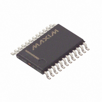
DS3881E+T&R/C Maxim Integrated Products, DS3881E+T&R/C Datasheet - Page 10

DS3881E+T&R/C
Manufacturer Part Number
DS3881E+T&R/C
Description
IC AUTO CCFL CTRLR 1CH 24-TSSOP
Manufacturer
Maxim Integrated Products
Type
CCFL Controllerr
Datasheet
1.DS3881EC.pdf
(28 pages)
Specifications of DS3881E+T&R/C
Frequency
40 ~ 100 kHz
Current - Supply
12mA
Voltage - Supply
4.75 V ~ 5.25 V
Operating Temperature
-40°C ~ 105°C
Package / Case
24-TSSOP
Lead Free Status / RoHS Status
Lead free / RoHS Compliant
Current - Output
-
Lead Free Status / Rohs Status
Details
Single-Channel Automotive CCFL Controller
The DS3881 incorporates SRAM-shadowed EEPROM
memory locations for all memory that needs to be
retained during power cycling. At power-up, SEEB (bit 7
of the BLC register) is low, which causes the shadowed
locations to act as ordinary EEPROM. Setting SEEB
high disables the EEPROM write function and causes
the shadowed locations to function as ordinary SRAM
cells. This allows an infinite number of write cycles with-
out causing EEPROM damage and also eliminates the
EEPROM write time, t
memory changes made when SEEB is set high are not
written to EEPROM, these changes are not retained
through power cycles, and the power-up EEPROM values
are the last values written with SEEB low.
The DS3881 provides two independent methods of
lamp dimming that can be combined to achieve a dim-
ming ratio of 300:1 or greater. The first method is
“burst” dimming, which uses a digital pulse-width-mod-
ulated (DPWM) signal (22.5Hz to 440Hz) to control the
lamp brightness. The second is “analog” dimming,
which is accomplished by adjusting the lamp current.
Burst dimming provides 128 linearly spaced brightness
steps. Analog dimming provides smaller substeps that
allow incremental brightness changes between burst
dimming steps. This ability is especially useful for low-
brightness dimming changes, where using burst dim-
ming alone would cause visible brightness step
changes. Analog dimming also allows the brightness to
be reduced below the minimum burst dimming level,
which provides for the maximum dimming range.
Burst dimming can be controlled using a user-supplied
analog voltage on the BRIGHT pin or through the I
interface. Analog dimming can only be controlled
through the I
require the complete dimming range and resolution capa-
bility of the DS3881, I
Burst dimming increases/decreases the brightness by
adjusting (i.e., modulating) the duty cycle of the DPWM
signal. During the high period of the DPWM cycle, the
lamps are driven at the selected lamp frequency
(40kHz to 100kHz) as shown in Figure 6. This part of
the cycle is called the “burst” period because of the
lamp frequency burst that occurs during this time.
During the low period of the DPWM cycle, the controller
disables the MOSFET gate drivers so the lamps are not
driven. This causes the current to stop flowing in the
lamps, but the time is short enough to keep the lamps
from de-ionizing.
10
____________________________________________________________________
2
C interface. Therefore, for applications that
2
C dimming control must be used.
W
from the write cycle. Because
Lamp Dimming Control
Shadowed EEPROM
Burst Dimming
2
C
The DS3881 can generate its own DPWM signal inter-
nally (set DPSS = 0 in CR1), which can then be
sourced to other DS3881s if required, or the DPWM sig-
nal can be supplied from an external source (set DPSS
= 1 in CR1). To generate the DPWM signal internally,
the DS3881 requires a clock (referred to as the dim-
ming clock) to set the DPWM frequency. The user can
supply the dimming clock by setting POSCS = 1 in CR1
and applying an external 22.5Hz to 440Hz signal at the
POSC pin, or the dimming clock can be generated by
the DS3881’s internal oscillator (set POSCS = 0 in
CR1), in which case the frequency is set by an external
resistor at the POSC pin. These two dimming clock
options are shown in Figure 3. Regardless of whether
the dimming clock is generated internally or sourced
externally, the POSCR0 and POSCR1 bits in CR2 must
be set to match the desired dimming clock frequency.
The internally generated DPWM signal can be provided
at the PSYNC I/O pin (set RGSO = 0 in CR1) for sourc-
ing to other DS3881s, if any, in the circuit. This allows
all DS3881s in the system to be synchronized to the
same DPWM signal. A DS3881 that is generating the
DPWM signal for other DS3881s in the system is
referred to as the DPWM source. When bringing in an
externally generated DPWM signal, either from another
DS3881 acting as a DPWM source or from some other
user-provided source, it is input into the PSYNC I/O pin
of the DS3881, and the receiving DS3881 is referred to
a DPWM receiver. In this mode, the BRIGHT and POSC
inputs are disabled and should be grounded (see
Figure 5).
When the DPWM signal is generated internally, its duty
cycle (and, thus, the lamp brightness) is controlled
either by a user-supplied analog voltage at the BRIGHT
input or through the I
PWM code in the BPWM register. When using the
BRIGHT pin to control burst dimming, a voltage of less
than 0.5V causes the DS3881 to operate with the mini-
mum burst duty cycle, providing the lowest brightness
setting, while any voltage greater than 2.0V causes a
100% burst duty cycle (i.e., lamps always being dri-
ven), which provides the maximum brightness. For volt-
ages between 0.5V and 2V, the duty cycle varies
linearly between the minimum and 100%. Writing a non-
zero PWM code to the BPWM register disables the
BRIGHT pin and enables I
Setting the 7-bit PWM code to 0000001b causes the
DS3881 to operate with the minimum burst duty cycle,
while a setting of 1111111b causes a 100% burst duty
cycle. For settings between these two codes, the duty
cycle varies linearly between the minimum and 100%.
2
C interface by varying the 7-bit
2
C burst dimming control.


