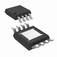
LM5111-2MY/NOPB National Semiconductor, LM5111-2MY/NOPB Datasheet - Page 3

LM5111-2MY/NOPB
Manufacturer Part Number
LM5111-2MY/NOPB
Description
IC MOSFET DRIVER DUAL 5A 8-EMSOP
Manufacturer
National Semiconductor
Datasheet
1.LM5111-1MYNOPB.pdf
(12 pages)
Specifications of LM5111-2MY/NOPB
Configuration
Low-Side
Input Type
Inverting
Delay Time
25ns
Current - Peak
5A
Number Of Configurations
2
Number Of Outputs
2
Voltage - Supply
3.5 V ~ 14 V
Operating Temperature
-40°C ~ 125°C
Mounting Type
Surface Mount
Package / Case
8-MSOP Exposed Pad, 8-HMSOP, 8-eMSOP
Number Of Drivers
2
Driver Configuration
Inverting
Driver Type
Low Side
Input Logic Level
TTL
Rise Time
25ns
Fall Time
25ns
Propagation Delay Time
40ns
Operating Supply Voltage (max)
14V
Peak Output Current
5mA
Output Resistance
1.4/30Ohm
Operating Supply Voltage (min)
3.5V
Operating Temp Range
-40C to 125C
Operating Temperature Classification
Automotive
Mounting
Surface Mount
Pin Count
8
Package Type
MSOP
Lead Free Status / RoHS Status
Lead free / RoHS Compliant
High Side Voltage - Max (bootstrap)
-
Lead Free Status / Rohs Status
Compliant
Other names
LM5111-2MY
LM5111-2MYTR
LM5111-2MYTR
V
V
I
CONTROL INPUTS
V
V
V
V
HYS
I
I
OUTPUT DRIVERS
R
R
I
I
CC
IL
IH
Source
Sink
CCR
CCH
IH
IL
thH
thL
OH
OL
Absolute Maximum Ratings
If Military/Aerospace specified devices are required,
please contact the National Semiconductor Sales Office/
Distributors for availability and specifications.
Electrical Characteristics
T
V
IN to V
Symbol
J
CC
= −40°C to +125°C, V
to V
EE
EE
V
V
(rising)
V
Hysteresis
V
Logic High
Logic Low
High Threshold
Low Threshold
Input Hysteresis
Input Current Low
Input Current High
Output Resistance High
Output Resistance Low
Peak Source Current
Peak Sink Current
CC
CC
CC
CC
Operating Range
Supply Current (I
Under Voltage Lockout
Under Voltage Lockout
Parameter
CC
= 12V, V
CC
)
EE
= 0V, No Load on OUT_A or OUT_B, unless otherwise specified.
−0.3V to 15V
−0.3V to 15V
V
V
IN_A = IN_B = 0V (5111-1)
IN_A = IN_B = V
IN_A = V
IN_A=IN_B=V
IN_B=V
IN_A=IN_B=V
IN_A=IN_B=V
IN_A=V
I
I
OUTA/OUTB = V
200 ns Pulsed Current
OUTA/OUTB = V
200 ns Pulsed Current
OUT
OUT
(Note 1)
CC
CC
−V
−V
= −10 mA (Note 2)
= + 10 mA (Note 2)
EE
EE
CC
CC
CC
(5111-3)
(5111-3)
, IN_B = 0V (5111-3)
Conditions
CC
CC
CC
CC
3
(5111-1-2-3)
(5111-2)
(5111-1)
CC
CC
(5111-2)
/2,
/2,
Storage Temperature Range, (T
Maximum Junction Temperature,
Operating Junction Temperature
ESD Rating
(T
J
(max))
Min
3.5
2.3
2.2
1.3
0.8
−1
10
−1
10
-1
1.75
1.35
Typ
230
400
2.9
0.1
0.1
0.1
1.4
18
18
30
1
1
1
3
5
STG
)
−55°C to +150°C
Max
3.5
0.8
2.2
2.0
2.5
14
25
25
50
2
2
2
1
1
1
www.national.com
+150°C
+125°C
Units
mV
mA
mV
2kV
µA
Ω
Ω
V
V
V
V
V
V
A
A


