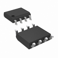
LM5111-1M/NOPB National Semiconductor, LM5111-1M/NOPB Datasheet

LM5111-1M/NOPB
Specifications of LM5111-1M/NOPB
*LM5111-1M/NOPB
LM5111-1M
Related parts for LM5111-1M/NOPB
LM5111-1M/NOPB Summary of contents
Page 1
... LM5111 Dual 5A Compound Gate Driver General Description The LM5111 Dual Gate Driver replaces industry standard gate drivers with improved peak output current and efficiency. Each “compound” output driver stage includes MOS and bipo- lar transistors operating in parallel that together sink more than 5A peak from capacitive loads ...
Page 2
... LM5111-2MX LM5111-3M LM5111-3MX LM5111-1MY MSOP8-EP LM5111-1MYX MSOP8-EP LM5111-2MY MSOP8-EP LM5111-2MYX MSOP8-EP LM5111-3MY MSOP8-EP LM5111-3MYX MSOP8-EP LM5111-4M LM5111-4MX LM5111-4MY MSOP8-EP LM5111-4MYX MSOP8-EP Pin Descriptions Pin Name Connect ‘A’ side control input 2 IN_A 3 VEE Ground reference for both inputs and outputs ‘B’ side control input ...
Page 3
... Absolute Maximum Ratings If Military/Aerospace specified devices are required, please contact the National Semiconductor Sales Office/ Distributors for availability and specifications Electrical Characteristics T = −40°C to +125° 12V Symbol Parameter V Operating Range Under Voltage Lockout CCR CC (rising Under Voltage Lockout CCH CC Hysteresis ...
Page 4
Symbol Parameter SWITCHING CHARACTERISTICS td1 Propagation Delay Time Low to High, IN rising (IN to OUT) td2 Propagation Delay Time High to Low, IN falling (IN to OUT) t Rise Time r t Fall Time f LATCHUP PROTECTION AEC - ...
Page 5
Typical Performance Characteristics Supply Current vs Frequency Rise and Fall Time vs Supply Voltage Supply Current vs Capacitive Load 20112310 Rise and Fall Time vs Temperature 20112312 5 20112311 20112313 www.national.com ...
Page 6
Rise and Fall Time vs Capacitive Load Delay Time vs Temperature www.national.com 20112314 20112316 UVLO Thresholds and Hysteresis vs Temperature 6 Delay Time vs Supply Voltage 20112315 RDSON vs Supply Voltage 20112317 20112318 ...
Page 7
... Block Diagram Block Diagram of LM5111 7 20112303 www.national.com ...
Page 8
... CC EE 3.0V. The LM5111-1, -2 and -3 devices hold both outputs in the low state in the under-voltage lockout (UVLO) condition. The LM5111-4 is distinguished from the LM5111-3 by the active high output state of OUT_A during UVLO. When VCC is less than the UVLO threshold voltage, OUT_A of the LM5111-4 will be locked in the high state while OUT_B will be disabled in the low state ...
Page 9
... FIGURE 2. The schematic above shows a conceptual diagram of the LM5111 output and MOSFET load. Q1 and Q2 are the switch- es within the gate driver the gate resistance of the G external MOSFET, and C is the equivalent gate capacitance IN of the MOSFET. The gate resistance Rg is usually very small and losses in it can be neglected ...
Page 10
Physical Dimensions NOTES: UNLESS OTHERWISE SPECIFIED 1. STANDARD LEAD FINISH TO BE 200 MICROINCHES/5.08 MICROMETERS MINIMUM LEAD/TIN(SOLDER) ON COPPER. 2. DIMENSION DOES NOT INCLUDE MOLD FLASH. 3. REFERENCE JEDEC REGISTRATION MS-012, VARIATION AA, DATED MAY 1990. www.national.com inches (millimeters) unless ...
Page 11
11 www.national.com ...
Page 12
... For more National Semiconductor product information and proven design tools, visit the following Web sites at: Products Amplifiers www.national.com/amplifiers Audio www.national.com/audio Clock Conditioners www.national.com/timing Data Converters www.national.com/adc Displays www.national.com/displays Ethernet www.national.com/ethernet Interface www.national.com/interface LVDS www.national.com/lvds Power Management www.national.com/power Switching Regulators www.national.com/switchers LDOs www ...


