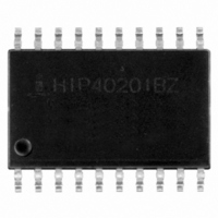
HIP4020IBZ Intersil, HIP4020IBZ Datasheet - Page 6

HIP4020IBZ
Manufacturer Part Number
HIP4020IBZ
Description
IC DRIVER FULL-BRIDGE 20-SOIC
Manufacturer
Intersil
Datasheet
1.HIP4020IBZ.pdf
(9 pages)
Specifications of HIP4020IBZ
Configuration
H Bridge
Input Type
Inverting and Non-Inverting
Delay Time
2.5µs
Current - Peak
625mA
Number Of Configurations
1
Number Of Outputs
4
Voltage - Supply
3 V ~ 12 V
Operating Temperature
-40°C ~ 85°C
Mounting Type
Surface Mount
Package / Case
20-SOIC (7.5mm Width)
Lead Free Status / RoHS Status
Lead free / RoHS Compliant
High Side Voltage - Max (bootstrap)
-
Available stocks
Company
Part Number
Manufacturer
Quantity
Price
Part Number:
HIP4020IBZ
Manufacturer:
HARRIS
Quantity:
20 000
Company:
Part Number:
HIP4020IBZT
Manufacturer:
Intersil
Quantity:
2 000
DIRECTION Input Control terminal. The MOS output transistor
pair chosen for conduction is determined by the logic level
applied to the DIRECTION control; resulting in either clockwise
(CW) or counter-clockwise (CCW) shaft rotation.
When the BRAKE terminal is switched high (while holding
the ENABLE input high), the gates of both Q2 and Q4 are
driven high. Current flowing through Q2 (from the motor
terminal OUTA) at the moment of Dynamic Braking will
continue to flow through Q2 to the V
connection, and then continue through diode D4 to the motor
terminal OUTB. As such, the resistance of the motor winding
(and the series-connected path) dissipates the kinetic
energy stored in the system. Reversing rotation, current
flowing through Q4 (from the motor terminal OUTB), at the
moment of Dynamic Braking, would continue to flow through
Q4 to the V
diode D2 to the motor terminal OUTA, to dissipate the stored
kinetic energy as previously described.
Where V
terminals for the Control Logic, the lowest practical supply
voltage for proper logic control should be no less than 2.0V.
The V
independent from V
SSA
DD
and V
FIGURE 4. EQUIVALENT CONTROL LOGIC A AND B SHOWN DRIVING THE OUTA AND OUTB OUTPUT DRIVERS
SSB
to V
(ENABLE)
(ENABLE)
(BRAKE)
(BRAKE)
and V
SS
SSB
(DIR)
(DIR)
ENA
ENB
are the Power Supply reference
SS
A1
A2
B1
B2
terminals are separate and
SSA
and may be more negative than the
tie, and then continue through
6
SSA
and V
SSB
external
HIP4020
V
supply level from V
than the Absolute Maximum Supply Voltage rating.
Terminals A1, B1, A2, B2, ENA and ENB are internally
connected to protection circuits intended to guard the CMOS
gate-oxides against damage due to electrostatic discharge.
(See Figure 3) Inputs ENA, ENB, A1, B1 A2 and B2 have
CD74HCT4000 Logic Interface Protection and Level
Converters for TTL or CMOS Input Logic. These inputs are
designed to typically provide ESD protection up to 2kV.
However, these devices are sensitive to electrostatic
discharge. Proper I.C. handling procedures should be
followed.
SS
FIGURE 3. LOGIC INPUT ESD INTERFACE PROTECTION
ground reference terminal. However, the maximum
INPUT
LIMIT
N-DR
LIMIT
LIMIT
LIMIT
P-DR
P-DR
N-DR
OT AND OC
OT AND OC
PROTECT
PROTECT
V
DD
DD
Q1
Q2
Q3
Q4
V
to V
V
V
V
SSB
DD
DD
SSA
SSA
D1
D2
D3
D4
or V
OUTA
OUTB
SSB
LEVEL
CONV.
must not be greater
December 20, 2005
FN3976.3


