SI9910DY-T1-E3 Vishay, SI9910DY-T1-E3 Datasheet
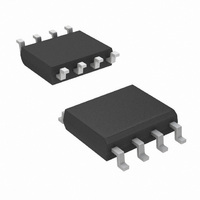
IC MOSFET DVR ADAPTIVE PWR 8SOIC

SI9910DY-T1-E3

Manufacturer Part Number
SI9910DY-T1-E3
Description
IC MOSFET DVR ADAPTIVE PWR 8SOIC
Manufacturer
Vishay
Type
High Sider
Datasheets

Specifications of SI9910DY-T1-E3

Configuration
High-Side
Input Type
Non-Inverting
Delay Time
120ns
Current - Peak
1A
Number Of Configurations
1
Number Of Outputs
1
High Side Voltage - Max (bootstrap)
500V
Voltage - Supply
10.8 V ~ 16.5 V
Operating Temperature
-40°C ~ 85°C
Mounting Type
Surface Mount
Package / Case
8-SOIC (3.9mm Width)
Rise Time
50 ns
Fall Time
35 ns
Supply Voltage (min)
10.8 V
Supply Current
0.5 mA
Maximum Power Dissipation
700 mW
Maximum Operating Temperature
+ 85 C
Mounting Style
SMD/SMT
Bridge Type
Half Bridge
Minimum Operating Temperature
- 40 C
Number Of Drivers
1
Device Type
MOSFET
Peak Output Current
1A
Input Delay
120ns
Output Delay
135ns
Supply Voltage Range
10.8V To 16.5V
Driver Case Style
SOIC
No. Of Pins
8
Operating Temperature Range
-40°C To +85°C
Lead Free Status / RoHS Status
Lead free / RoHS Compliant
Lead Free Status / RoHS Status
Lead free / RoHS Compliant, Lead free / RoHS Compliant
Other names
SI9910DY-T1-E3TR

Available stocks

Company
Part Number
Manufacturer
Quantity
Price
Part Number:
SI9910DY-T1-E3
Manufacturer:
TI
Quantity:
87
Part Number:
SI9910DY-T1-E3
Manufacturer:
VISHAY/威世
Quantity:
20 000
Company:
Part Number:
SI9910DY-T1-E3
Quantity:
11 589
The Si9910 is the first of a new generation of “adaptive” power
MOSFET gate drivers.
protection for the power MOSFET switching element while
allowing direct control of high-voltage switching from logic
signals. To achieve this protection, the Si9910 monitors the
power MOSFET’s operating conditions through feedback
loops and alters its output characteristics.
The Si9910 adaptive driver allows the system designer to take
full advantage of the increased performance and efficiency of
power MOSFETs. Previous gate-drive techniques required
designing a system for safe operation under worst-case
conditions, even those which occur infrequently. Thus, these
systems operated
optimum conditions with considerable performance and
efficiency penalties. The Si9910, however, prevents power
MOSFET destruction under worst-case operating conditions
without compromising system performance and efficiency
during normal operation.
The Si9910 is a single-channel, non-inverting CMOS driver
with a low-impedance, emitter-follower output and a Schmidt
trigger input (see Figure 1). To take full advantage of the
efficiency offered by the power MOSFET’s capacitive input
impedance characteristic, the Si9910 was designed to have
Document Number: 70579
15-Feb-94
Si9910 Adaptive Power MOSFET Driver Improves Performance in
INPUT
V
DD
most of the time
These adaptive drivers provide
V
High-Voltage Half-Bridge Applications
DS
Delay
2 s
Undervoltage/
Overcurrent
Protection
under less than
FIGURE 1. Si9910 Block Diagram
V
SS
extremely low quiescent current and low output gate-drive
impedance.
A “power IC” process incorporating CMOS, DMOS, and
bipolar device technologies are employed to optimize the
Si9910 driver characteristics.
section requires a maximum quiescent current of 1 A (with
the output high and the power MOSFET turned on), while the
emitter-follower output stage is capable of delivering 1 A of
peak current to quickly charge and discharge MOSFET gate
capacitance.
eliminates shoot-through and quiescent bias current losses in
the low-impedance output stage.
One potently damaging characteristic of a high-voltage
motor-drive circuit is inductive flyback energy. Damaging
voltages can result when inductor drive current is
interrupted, unless some method is used to clamp the voltage
and “free wheel” the inductive flyback energy (see Figure 2).
For example, in unipolar motor-drive techniques, the flyback
voltage is often clamped with a discrete diode to the motor
supply or with a Zener diode to ground. One benefit that power
MOSFETs offer is their intrinsic diodes which can serve as
reliable and efficient voltage clamps.
PULL-DOWN
Using a bipolar emitter-follower output
PULL-UP
DRAIN
I
SENSE
* Typical Values
www.vishay.com FaxBack 408-970-5600
*250
*100 k
R3
R2
C1
The driver’s CMOS
Vishay Siliconix
*2 to 5 pF
*0.1
R1
AN705
logic
1

Related parts for SI9910DY-T1-E3

SI9910DY-T1-E3 Summary of contents

Page 1

... Zener diode to ground. One benefit that power MOSFETs offer is their intrinsic diodes which can serve as reliable and efficient voltage clamps. PULL-DOWN V SS FIGURE 1. Si9910 Block Diagram AN705 Vishay Siliconix The driver’s CMOS logic R3 *100 k C1 DRAIN * PULL-UP R2 *250 I SENSE R1 *0.1 * Typical Values www.vishay.com FaxBack 408-970-5600 1 ...

Page 2

... The power switching arrangement most commonly used is the half-bridge configuration. half-bridge, each motor winding is connected to a common node between switching devices that can connect it to either the motor supply voltage or to the motor supply return. In www.vishay.com FaxBack 408-970-5600 2 DRAIN PULL-UP PULL-DOWN ...

Page 3

... The only 1 Addressing this issue in high-voltage (500 V) applications is a new line of MOSPOWER transistors from Vishay Siliconix with intrinsic diode recovery times rivaling discrete fast-recovery diodes. However, even these fast-recovery diodes don’t solve all the problems associated with flyback energy and diode recovery ...

Page 4

... INPUT Figure 4. Controlling di/dt via MOSFET Gate Drive Impedance The Si9910 I input can be used in conjunction with a SENSE very low-value external sense resistor to directly limit the maximum peak current (Figure 5). Figure 6 illustrates a www.vishay.com FaxBack 408-970-5600 4 DRAIN PULL-UP PULL-DOWN I SENSE (Q1 (Q2) rr Diode Recovery ...

Page 5

... Document Number: 70579 15-Feb-94 DRAIN Overcurrent PULL-UP Protection PULL-DOWN A V (Q1 (Q2 (Q1 (Q1 Figure 5. Limiting Peak Current R2 R SENSE AN705 Vishay Siliconix V+ Q2 Motor Winding and SENSE R SENSE (R1) I PEAK (Not to Scale) I MOTOR DRAIN C1 PULL-UP R2 PULL-DOWN Figure 7. Simplified dv/dt Feedback Circuit www.vishay.com FaxBack 408-970-5600 5 ...

Page 6

... www.vishay.com FaxBack 408-970-5600 6 the common base of the emitter-follower stage changes from a low to a high level, the output follows, turning the power SENSE MOSFET on. As the power MOSFET switches voltage across its drain-source decreases rapidly. The rate of dv/dt will depend on all of the conditions described earlier that are associated with diode reverse recovery ...

Page 7

... Figure 9 illustrates both the charge pump and bootstrap circuits used in conjunction with an Si9910 in a high- side driver application. www.vishay.com FaxBack 408-970-5600 AN705 Vishay Siliconix ...

Page 8

... V drain input is not in use, it must be left open. When the I input is not in use, it should be shorted to V Using surface-mount driver ICs, such as the Si9910DY shown in Figure 11 substrate with power MOSFET chips holds great promise for next-generation motor drives. The power MOSFET can be mounted directly on a substrate with good ...

Page 9

... Document Number: 70579 15-Feb-94 DRAIN PULL-UP PULL-DOWN I SENSE (Q1 (Q2) rr (Q1) (Q1 Figure 10. All Feedback Options Active INPUT DRAIN of power Figure 11. Si9910DY and Si9910DJ Package Pin-Outs AN705 Vishay Siliconix V+ Q2 Motor Winding and Limit PEAK (Not to Scale) I MOTOR PULL- ...

Related keywords