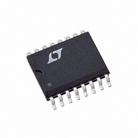
LT1158ISW#TR Linear Technology, LT1158ISW#TR Datasheet - Page 10

LT1158ISW#TR
Manufacturer Part Number
LT1158ISW#TR
Description
IC DRIVER PWR MOSFET N-CH 16SOIC
Manufacturer
Linear Technology
Datasheet
1.LT1158CNPBF.pdf
(22 pages)
Specifications of LT1158ISW#TR
Configuration
Half Bridge
Input Type
PWM
Current - Peak
500mA
Number Of Configurations
1
Number Of Outputs
2
High Side Voltage - Max (bootstrap)
56V
Voltage - Supply
5 V ~ 30 V
Operating Temperature
-40°C ~ 85°C
Mounting Type
Surface Mount
Package / Case
16-SOIC (0.300", 7.5mm Width)
Lead Free Status / RoHS Status
Contains lead / RoHS non-compliant
Delay Time
-
Available stocks
Company
Part Number
Manufacturer
Quantity
Price
LT1158
APPLICATIONS INFORMATION
If individual gate decoupling resistors are used, the gate
feedback pins can be connected to any one of the gates.
Driving multiple MOSFETs in parallel may restrict the
operating frequency at high supply voltages to prevent
over-dissipation in the LT1158 (see Gate Charge and
Driver Dissipation below). When the total gate capacitance
exceeds 10,000pF on the top side, the bootstrap capacitor
should be increased proportionally above 0.1μF .
Gate Charge and Driver Dissipation
A useful indicator of the load presented to the driver by a
power MOSFET is the total gate charge Q
the additional charge required by the gate-to-drain swing. Q
is usually specifi ed for V
When the supply current is measured in a switching ap-
plication, it will be larger than given by the DC electrical
characteristics because of the additional supply current
associated with sourcing the MOSFET gate charge:
The actual increase in supply current is slightly higher
due to LT1158 switching losses and the fact that the gates
are being charged to more than 10V. Supply current vs
switching frequency is given in the Typical Performance
Characteristics.
The LT1158 junction temperature can be estimated by
using the equations given in Note 1 of the electrical char-
acteristics. For example, the LT1158SI is limited to less
than 25mA from a 24V supply:
In order to prevent the maximum junction temperature
from being exceeded, the LT1158 supply current must
be checked with the actual MOSFETs operating at the
maximum switching frequency.
10
T
I
SUPPLY
J
= 85°C + (25mA • 24V • 110°C/W)
= 151°C exceeds absolute maximum
=
I
DC
+
⎛
⎝ ⎜
dQ
dt
G
GS
⎞
⎠ ⎟
TOP
= 10V and V
+
⎛
⎝ ⎜
dQ
dt
G
DS
⎞
⎠ ⎟
G
BOTTO
, which includes
= 0.8V
M M
DS(MAX)
G
.
MOSFET Gate Drive Protection
For supply voltages of over 8V, the LT1158 will protect
standard N-channel MOSFETs from under or overvoltage
gate drive conditions for any input duty cycle including
DC. Gate-to-source Zener clamps are not required and
not recommended since they can reduce operating
efficiency.
A discontinuity in tracking between the output pulse
width and input pulse width may be noted as the top side
MOSFET approaches 100% duty cycle. As the input low
signal becomes narrower, it may become shorter than
the time required to recharge the bootstrap capacitor to
a safe voltage for the top side driver. Below this duty cycle
the output pulse width will stop tracking the input until
the input low signal is <100ns, at which point the output
will jump to the DC condition of top MOSFET “on” and
bottom MOSFET “off.”
Low Voltage Operation
The LT1158 can operate from 5V supplies (4.5V min) and
in 6V battery-powered applications by using logic-level
N-channel power MOSFETs. These MOSFETs have 2V
maximum threshold voltages and guaranteed R
at V
CMOS drivers, does not degrade at low supply voltages.
For operation down to 4.5V, the boost pin should be con-
nected as shown in Figure 2 to maximize gate drive to the
top side MOSFET. Supply voltages over 10V should not
be used with logic-level MOSFETs because of their lower
maximum gate-to-source voltage rating.
GS
= 4V. The switching speed of the LT1158, unlike
LT1158
BOOST DR
N.C.
T GATE DR
T SOURCE
T GATE FB
Figure 2. Low Voltage Operation
BOOST
D1: LOW-LEAKAGE SCHOTTKY
BAT85 OR EQUIVALENT
D1
0.1μF
5V
LOGIC-LEVEL
MOSFET
+
DS(ON)
LT1158 F02
limits
1158fb


