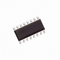
HCPL-316J#500 Avago Technologies US Inc., HCPL-316J#500 Datasheet - Page 30

HCPL-316J#500
Manufacturer Part Number
HCPL-316J#500
Description
OPTOCOUPLER 1CH 2.5A 16-SOIC
Manufacturer
Avago Technologies US Inc.
Datasheet
1.HCPL-316J-500E.pdf
(33 pages)
Specifications of HCPL-316J#500
Package / Case
16-SOIC (0.300", 7.5mm Width)
Configuration
High-Side
Input Type
Differential
Delay Time
300ns
Current - Peak
2.5A
Number Of Configurations
1
Number Of Outputs
1
Voltage - Supply
4.5 V ~ 5.5 V
Operating Temperature
-40°C ~ 100°C
Mounting Type
Surface Mount
Lead Free Status / RoHS Status
Contains lead / RoHS non-compliant
High Side Voltage - Max (bootstrap)
-
Lead Free Status / RoHS Status
Lead free / RoHS Compliant, Contains lead / RoHS non-compliant
Available stocks
Company
Part Number
Manufacturer
Quantity
Price
As an example, the total input and output power dis-
sipation can be calculated given the following condi-
tions:
Step 1: Calculate R
To find the peak charging l
initially charged the steady-state value of V
apply the following relationship:
R
(Note from Figure 76 that the real value of I
calculated from the simple model shown.)
Step 2: Calculate total power dissipation in the HCPL-316J:
The HCPL-316J total power dissipation (P
the sum of the input-side power (P
power (P
where,
Figure 76. Typical peak I
HCPL-316J output driving an IGBT rated at 600 V/100 A.
30
G
P
P
• I
• V
• V
• f
P
= ——————————
= ——————————
= 10.25 :
≈ 10.5 : (for a 1% resistor)
I
O
= —————————
T
-1
-2
-3
[V
4
3
2
1
0
18 V – 1 V – (1.5 V + (-5 V))
= I
ON, MAX
CARRIER
[V
= P
= P
MAX. I
CC2
EE
0
OH
= I
CC2
CC1
= -5 V
20
I
O(BIAS)
@650 μA – (V
O
CC2
+ P
= 18 V
):
ON
– 1 – (V
* V
40 60 80
(V
O
= 15 kHz
* (V
, I
CC2
~ 2.0 A
CC1
OFF
+ P
I
I
2.0 A
OL,PEAK
OL,PEAK
CC2
/ V
G
I
I
OFF
ON
v . GATE RESISTANCE
minimum from I
OL
O,SWTICH
Rg (Ω)
EE2
ON
100
–V
(MAX.)
(MAX.)
+ V
and I
= 25 V / 5 V
OL
EE
120
EE
+V
) + E
OFF
140
)]
EE
currents vs. Rg (for
OL
160 180
SWITCH
)]
assume that the gate is
OL
peak specification:
200
* f
OL
I
) and output-side
SWITCH
may vary from the value
T
) is equal to
EE
. Therefore
Figure 77. Switching energy plot for calculating average Pswitch
(for HCPL-316J output driving an IGBT rated at 600 V/100 A).
P
PL-316J due to biasing the device.
P
PL-316J due to charging and discharging power device
gate.
E
to switching of the power device over one switching
cycle (μJ/cycle).
f
For R
= 6.05 μJ. Assume a worst-case average I
(which is given by the average of I
larly the average I
P
P
Step 3: Compare the calculated power dissipation with the abso-
lute maximum values for the HCPL-316J:
For the example,
Therefore, the power dissipation absolute maximum
rating has not been exceeded for the example.
Please refer to the following Thermal Model section for
an explanation on how to calculate the maximum junc-
tion temperature of the HCPL-316J for a given PC board
layout configuration.
SWITCH
SWITCH
I
O
O(BIAS)
O(SWITCH)
= 16.5 mA * 5.5 V = 90.8 mW
= P
= 5.5 mA * (18 V – (–5 V)) + 6.051 μJ * 15 kHz
= 126.5 mW + 90.8 mW
= 217.3 mW
P
P
SWITCHING ENERGY v . GATE RESISTANCE
I
O
9
8
7
6
5
4
3
2
1
0
G
= 90.8 mW < 150 mW (abs. max.)
OK
0
= 10.5, the value read from Figure 77 is E
O(BIAS)
= 217.3 mW < 600 mW (abs. max.)
OK
= average carrier signal frequency.
= steady-state power dissipation in the HC-
= Average Energy dissipated in HCPL-316J due
= transient power dissipation in the HC-
(V
50
+ P
CC2
E
O,SWITCH
/ V
(Qg = 650 nC)
CC2
Rg (Ω)
EE2
100
= 5.5 mA.
= 25 V / 5 V
150
CC1H
200
and I
CC1
CC1L
= 16.5 mA
SWITCH
). Simi-


