ISL6609ACRZ-T Intersil, ISL6609ACRZ-T Datasheet - Page 7
ISL6609ACRZ-T
Manufacturer Part Number
ISL6609ACRZ-T
Description
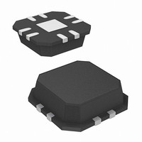
IC MOSFET DRVR SYNC BUCK 8-QFN
Manufacturer
Intersil
Datasheet
1.ISL6609AIRZ-TK.pdf
(12 pages)
Specifications of ISL6609ACRZ-T
Configuration
High and Low Side, Synchronous
Input Type
PWM
Delay Time
18ns
Current - Peak
2A
Number Of Configurations
1
Number Of Outputs
2
Voltage - Supply
4.5 V ~ 5.5 V
Operating Temperature
0°C ~ 70°C
Mounting Type
Surface Mount
Package / Case
8-VQFN
Lead Free Status / RoHS Status
Lead free / RoHS Compliant
High Side Voltage - Max (bootstrap)
-
Available stocks
Company
Part Number
Manufacturer
Quantity
Price

Part Number:
ISL6609ACRZ-T
Manufacturer:
INTERSIL
Quantity:
20 000


Timing Diagram
Operation and Adaptive Shoot-Through Protection
Designed for high speed switching, the ISL6609, ISL6609A
MOSFET driver controls both high-side and low-side N-
Channel FETs from one externally provided PWM signal.
A rising transition on PWM initiates the turn-off of the lower
MOSFET (see “Timing Diagram”). After a short propagation
delay [t
[t
page 5. Adaptive shoot-through circuitry monitors the
LGATE voltage and turns on the upper gate following a short
delay time [t
~1V. The upper gate drive then begins to rise [t
upper MOSFET turns on.
A falling transition on PWM indicates the turn-off of the upper
MOSFET and the turn-on of the lower MOSFET. A short
propagation delay [t
gate begins to fall [t
monitors the UGATE-PHASE voltage and turns on the lower
MOSFET a short delay time, t
MOSFET’s gate voltage drops below 1V. The lower gate then
rises [t
prevent both the lower and upper MOSFETs from conducting
simultaneously (shoot-through), while adapting the dead
time to the gate charge characteristics of the MOSFETs
being used.
This driver is optimized for voltage regulators with large step
down ratio. The lower MOSFET is usually sized larger
compared to the upper MOSFET because the lower MOSFET
conducts for a longer time during a switching period. The
lower gate driver is therefore sized much larger to meet this
application requirement. The 0.4Ω ON-resistance and 4A sink
PWM
UGATE
LGATE
FL
t
PDLL
] are provided in the “Electrical Specifications” table on
RL
PDLL
], turning on the lower MOSFET. These methods
PDHU
], the lower gate begins to fall. Typical fall times
t
] after the LGATE voltage drops below
PDHU
FU
PDLU
1V
]. The adaptive shoot-through circuitry
t
] is encountered before the upper
RU
PDHL
7
t
PDLU
, after the upper
RU
t
PDHL
1V
] and the
FIGURE 1. TIMING DIAGRAM
ISL6609, ISL6609A
2.5V
t
RL
t
FL
current capability enable the lower gate driver to absorb the
current injected into the lower gate through the drain-to-gate
capacitor of the lower MOSFET and help prevent shoot
through caused by the self turn-on of the lower MOSFET due
to high dV/dt of the switching node.
Three-State PWM Input
A unique feature of the ISL6609, ISL6609A is the adaptable
three-state PWM input. Once the PWM signal enters the
shutdown window, either MOSFET previously conducting is
turned off. If the PWM signal remains within the shutdown
window for longer than the gate turn-off propagation delay of
the previously conducting MOSFET, the output drivers are
disabled and both MOSFET gates are pulled and held low.
The shutdown state is removed when the PWM signal moves
outside the shutdown window. The PWM rising and falling
thresholds outlined in the “Electrical Specifications” table on
page 5 determine when the lower and upper gates are
enabled. During normal operation in a typical application, the
PWM rise and fall times through the shutdown window should
not exceed either output’s turn-off propagation delay plus the
MOSFET gate discharge time to ~1V. Abnormally long PWM
signal transition times through the shutdown window will
simply introduce additional dead time between turn off and
turn on of the synchronous bridge’s MOSFETs. For optimal
performance, no more than 100pF parasitic capacitive load
should be present on the PWM line of ISL6609, ISL6609A
(assuming an Intersil PWM controller is used).
Bootstrap Considerations
This driver features an internal bootstrap diode. Simply
adding an external capacitor across the BOOT and PHASE
pins completes the bootstrap circuit. The ISL6609A’s internal
t
TSSHD
t
PTS
t
RU
t
TSSHD
t
FU
t
PTS
April 27, 2009
FN9221.2
Related parts for ISL6609ACRZ-T
Image
Part Number
Description
Manufacturer
Datasheet
Request
R

Part Number:
Description:
Synchronous Rectified MOSFET Driver
Manufacturer:
Intersil Corporation
Datasheet:

Part Number:
Description:
Synchronous Rectified MOSFET Driver
Manufacturer:
INTERSIL [Intersil Corporation]
Datasheet:
Part Number:
Description:
Intersil Corporation [CMOS Serial Controller Interface]
Manufacturer:
Intersil Corporation
Datasheet:
Part Number:
Description:
Manufacturer:
Intersil Corporation
Datasheet:
Part Number:
Description:
357-036-542-201 CARDEDGE 36POS DL .156 BLK LOPRO
Manufacturer:
Intersil Corporation
Datasheet:
Part Number:
Description:
1024-Word x 4-Bit LSI Static RAM
Manufacturer:
Intersil Corporation
Datasheet:
Part Number:
Description:
General Purpose NPN Transistor Arrays FN341.4
Manufacturer:
Intersil Corporation
Datasheet:
Part Number:
Description:
CMOS 16-Bit Microprocessor
Manufacturer:
Intersil Corporation
Datasheet:
Part Number:
Description:
Manufacturer:
Intersil Corporation
Datasheet:
Part Number:
Description:
Manufacturer:
Intersil Corporation
Datasheet:
Part Number:
Description:
Manufacturer:
Intersil Corporation
Datasheet:
Part Number:
Description:
Manufacturer:
Intersil Corporation
Datasheet:
Part Number:
Description:
CMOS 6-Bit Latch and Decoder Memory Interfaces
Manufacturer:
Intersil Corporation
Datasheet:
Part Number:
Description:
CA3046General Purpose NPN Transistor Arrays
Manufacturer:
Intersil Corporation
Datasheet:
Part Number:
Description:
Manufacturer:
Intersil Corporation
Datasheet: