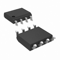
LM5100AMX/NOPB National Semiconductor, LM5100AMX/NOPB Datasheet - Page 13

LM5100AMX/NOPB
Manufacturer Part Number
LM5100AMX/NOPB
Description
IC DVR HALF-BRIDGE HV 8-SOIC
Manufacturer
National Semiconductor
Datasheet
1.LM5101CSDNOPB.pdf
(18 pages)
Specifications of LM5100AMX/NOPB
Configuration
High and Low Side, Synchronous
Input Type
Non-Inverting
Delay Time
20ns
Current - Peak
3A
Number Of Configurations
1
Number Of Outputs
2
High Side Voltage - Max (bootstrap)
118V
Voltage - Supply
9 V ~ 14 V
Operating Temperature
-40°C ~ 125°C
Mounting Type
Surface Mount
Package / Case
8-SOIC (3.9mm Width)
Number Of Drivers
2
Driver Configuration
Non-Inverting
Driver Type
High and Low Side
Input Logic Level
CMOS
Rise Time
430ns
Fall Time
260ns
Propagation Delay Time
20ns
Operating Supply Voltage (max)
14V
Peak Output Current
3mA
Operating Supply Voltage (min)
9V
Turn Off Delay Time
1ns
Turn On Delay Time (max)
1ns
Operating Temp Range
-40C to 125C
Operating Temperature Classification
Automotive
Mounting
Surface Mount
Pin Count
8
Package Type
SOIC N
Lead Free Status / RoHS Status
Lead free / RoHS Compliant
Other names
LM5100AMX
Available stocks
Company
Part Number
Manufacturer
Quantity
Price
Company:
Part Number:
LM5100AMX/NOPB
Manufacturer:
ROHM
Quantity:
6 262
Part Number:
LM5100AMX/NOPB
Manufacturer:
TI/德州仪器
Quantity:
20 000
Diode Power Dissipation V
= 50V
Power Dissipation Considerations
IN
The total IC power dissipation is the sum of the gate driver
losses and the bootstrap diode losses. The gate driver losses
are related to the switching frequency (f), output load capac-
itance on LO and HO (C
), and supply voltage (VDD) and can
L
be roughly calculated as:
P
= 2 • f • C
• V
2
DGATES
L
DD
There are some additional losses in the gate drivers due to
the internal CMOS stages used to buffer the LO and HO out-
puts. The following plot shows the measured gate driver
power dissipation versus frequency and load capacitance. At
higher frequencies and load capacitance values, the power
dissipation is dominated by the power losses driving the out-
put loads and agrees well with the above equation. This plot
can be used to approximate the power losses due to the gate
drivers.
20203106
Gate Driver Power Dissipation (LO + HO)
V
= 12V, Neglecting Diode Losses
DD
20203105
The bootstrap diode power loss is the sum of the forward bias
power loss that occurs while charging the bootstrap capacitor
and the reverse bias power loss that occurs during reverse
recovery. Since each of these events happens once per cycle,
the diode power loss is proportional to frequency. Larger ca-
pacitive loads require more energy to recharge the bootstrap
capacitor resulting in more losses. Higher input voltages
(V
) to the half bridge result in higher reverse recovery loss-
IN
es. The following plot was generated based on calculations
and lab measurements of the diode recovery time and current
under several operating conditions. This can be useful for ap-
proximating the diode power dissipation.
The total IC power dissipation can be estimated from the pre-
vious plots by summing the gate drive losses with the boot-
strap diode losses for the intended application.
13
www.national.com


