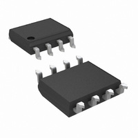
LM5100AMX/NOPB National Semiconductor, LM5100AMX/NOPB Datasheet - Page 7

LM5100AMX/NOPB
Manufacturer Part Number
LM5100AMX/NOPB
Description
IC DVR HALF-BRIDGE HV 8-SOIC
Manufacturer
National Semiconductor
Datasheet
1.LM5101CSDNOPB.pdf
(18 pages)
Specifications of LM5100AMX/NOPB
Configuration
High and Low Side, Synchronous
Input Type
Non-Inverting
Delay Time
20ns
Current - Peak
3A
Number Of Configurations
1
Number Of Outputs
2
High Side Voltage - Max (bootstrap)
118V
Voltage - Supply
9 V ~ 14 V
Operating Temperature
-40°C ~ 125°C
Mounting Type
Surface Mount
Package / Case
8-SOIC (3.9mm Width)
Number Of Drivers
2
Driver Configuration
Non-Inverting
Driver Type
High and Low Side
Input Logic Level
CMOS
Rise Time
430ns
Fall Time
260ns
Propagation Delay Time
20ns
Operating Supply Voltage (max)
14V
Peak Output Current
3mA
Operating Supply Voltage (min)
9V
Turn Off Delay Time
1ns
Turn On Delay Time (max)
1ns
Operating Temp Range
-40C to 125C
Operating Temperature Classification
Automotive
Mounting
Surface Mount
Pin Count
8
Package Type
SOIC N
Lead Free Status / RoHS Status
Lead free / RoHS Compliant
Other names
LM5100AMX
Available stocks
Company
Part Number
Manufacturer
Quantity
Price
Company:
Part Number:
LM5100AMX/NOPB
Manufacturer:
ROHM
Quantity:
6 262
Part Number:
LM5100AMX/NOPB
Manufacturer:
TI/德州仪器
Quantity:
20 000
t
t
PW
BS
Symbol
Note 1: Absolute Maximum Ratings indicate limits beyond which damage to the component may occur. Operating Ratings are conditions under which operation
of the device is guaranteed. Operating Ratings do not imply guaranteed performance limits. For guaranteed performance limits and associated test conditions,
see the Electrical Characteristics tables.
Note 2: The human body model is a 100 pF capacitor discharged through a 1.5kΩ resistor into each pin. 2 kV for all pins except Pin 2, Pin 3 and Pin 4 which are
rated at 1000V for HBM and 100V for MM.
Note 3: 4 layer board with Cu finished thickness 1.5/1/1/1.5 oz. Maximum die size used. 5x body length of Cu trace on PCB top. 50 x 50mm ground and power
planes embedded in PCB. See Application Note AN-1187.
Note 4: Min and Max limits are 100% production tested at 25°C. Limits over the operating temperature range are guaranteed through correlation using Statistical
Quality Control (SQC) methods. Limits are used to calculate National’s Average Outgoing Quality Level (AOQL).
Note 5: The θ
Note 6: In the application the HS node is clamped by the body diode of the external lower N-MOSFET, therefore the HS node will generally not exceed -1V.
However, in some applications, board resistance and inductance may result in the HS node exceeding this stated voltage transiently. If negative transients occur,
the HS voltage must never be more negative than VDD-15V. For example if VDD = 10V, the negative transients at HS must not exceed -5V.
Typical Performance Characteristics
Minimum Input Pulse Width that Changes
the Output
Bootstrap Diode Reverse Recovery Time I
JA
is not a given constant for the package and depends on the printed circuit board design and the operating environment.
Sink Current vs Output Voltage
Peak Sourcing Current vs VDD
Parameter
20203129
20203127
I
F
R
= 100 mA,
= 100 mA
Conditions
7
Source Current vs Output Voltage
Peak Sinking Current vs VDD
Min
Typ
50
37
Max
20203130
20203128
www.national.com
Units
ns
ns


