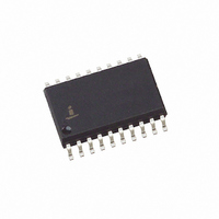
HIP4020IB Intersil, HIP4020IB Datasheet - Page 4

HIP4020IB
Manufacturer Part Number
HIP4020IB
Description
IC DRIVER FULL-BRIDGE 20-SOIC
Manufacturer
Intersil
Datasheet
1.HIP4020IBZ.pdf
(9 pages)
Specifications of HIP4020IB
Configuration
H Bridge
Input Type
Inverting and Non-Inverting
Delay Time
2.5µs
Current - Peak
625mA
Number Of Configurations
1
Number Of Outputs
4
Voltage - Supply
3 V ~ 12 V
Operating Temperature
-40°C ~ 85°C
Mounting Type
Surface Mount
Package / Case
20-SOIC (7.5mm Width)
Supply Voltage Min
3V
Supply Voltage Max
12V
Output Current
15mA
Driver Case Style
SOIC
Sink Output Current
15mA
Device Type
Power
Termination Type
SMD
No. Of Pins
20
Rohs Compliant
No
Peak Reflow Compatible (260 C)
No
Lead Free Status / RoHS Status
Contains lead / RoHS non-compliant
High Side Voltage - Max (bootstrap)
-
Available stocks
Company
Part Number
Manufacturer
Quantity
Price
Company:
Part Number:
HIP4020IB
Manufacturer:
HARRIS
Quantity:
32
Part Number:
HIP4020IB
Manufacturer:
INTERSIL
Quantity:
20 000
Part Number:
HIP4020IBZ
Manufacturer:
HARRIS
Quantity:
20 000
Company:
Part Number:
HIP4020IBZT
Manufacturer:
Intersil
Quantity:
2 000
Electrical Specifications
Pin Descriptions
Thermal Shutdown
Response Time: V
Turn-On: Prop Delay
Rise Time
Turn-Off: Prop Delay
Fall Time
PIN NUMBER
12, 19
14, 17
8, 5
9, 3
7, 4
15
16
6
2
PARAMETER
EN
to V
OUTA, OUTB
ENA, ENB
SYMBOL
OUT
A1, B1
A2, B2
V
V
V
V
ILF
SSA
SSB
DD
SS
4
T
A
= 25°C, V
Positive Power Supply pins; internally common and externally connect to the same Positive Supply (V+).
Negative Power Supply pin; Negative or Ground return for Switch Driver A; externally connect to the Supply
(V-).
Negative Power Supply pin; Negative or Ground return for Switch Driver B; externally connect to the Supply
(V-).
Common Ground pin for the Input Logic Control circuits. May be used as a common ground with V SSA and
V
Input pins used to control the direction of output load current to/from OUTA and OUTB, respectively. When
connected, A1 and B1 can be controlled from the same logic signal to change the directional rotation of a
motor.
Input pins used to force a low state on OUTA and OUTB, respectively. When connected, A2 and B2 can be
controlled from the same logic signal to activate Dynamic Braking of a motor.
Input pins used to Enable Switch Driver A and Switch Driver B, respectively. When Low, the respective
output is in a high impedance (Z) off-state. Since each Switch Driver is independently controlled, OUTA and
OUTB may be a separately PWM controlled as Half H-Switch Drivers.
Respectively, Switch Driver A and Switch Driver B Output pins.
Current Limiting Fault Output Flag pin; when in a high logic state, signifies that Switch Driver A or B or both
are in a Current Limiting Fault Mode.
SSB.
SYMBOL
DD
t
t
T
PLH
PHL
SD
t
t
r
f
= +5V, V
I
O
SSA
= 0.5A (Note 3)
HIP4020
= V
SSB
TEST CONDITIONS
= V
SS
= 0V, Unless Otherwise Specified (Continued)
DESCRIPTION
MIN
-
-
-
-
-
TYP
145
2.5
0.1
0.1
4
MAX
-
-
-
-
-
December 20, 2005
UNITS
FN3976.3
°C
µs
µs
µs
µs


