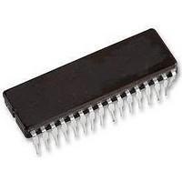
MC33395TEWR2 Freescale Semiconductor, MC33395TEWR2 Datasheet

MC33395TEWR2
Specifications of MC33395TEWR2
Related parts for MC33395TEWR2
MC33395TEWR2 Summary of contents
Page 1
... Pb-Free Packaging Designated by Suffix Code EW V PWR MCU 3 * This document contains certain information on a new product. Specifications and information herein are subject to change without notice. © Freescale Semiconductor, Inc., 2007. All rights reserved. ≤ supply. IGN Power MOSFETs MC33395DWB/R2 MC33395EW/R2 MCZ33395EW/R2 MC33395TDWB/R2 MC33395TEW/R2 33395 VIGNP ...
Page 2
... Drive Limiting Control Control Logic Gate Logic Drive Gate Circuits Drive Circuits Overtemperature Shutdown Shutdown CP1H CP1L Charge Charge Pump Pump CP2H CP2L CPRES VGDH VIGNP GDH1 GDH2 GDH3 SRC1 SRC2 SRC3 GDL1 GDL2 GDL3 Analog Integrated Circuit Device Data Freescale Semiconductor ...
Page 3
... GDL3 Output 15 PGND Ground 16 Test N/A 17 -ISENS Input 18 +ISENS Input 19 AGND Ground 20 VDD Power 21 PWM Input Analog Integrated Circuit Device Data Freescale Semiconductor PIN CONNECTIONS CP2H 1 32 CPRES 2 31 VIGN 3 30 VGDH 4 29 VIGNP 5 28 SRC1 6 27 GDH1 7 26 GDL1 8 25 ...
Page 4
... External Pump Capacitor Input from external pump capacitor for charge pump and secondary pins External Pump Capacitor Input from external reservoir, external pump capacitors for charge pump, Charge Pump and secondary pins Capacitor page 9. Definition Analog Integrated Circuit Device Data Freescale Semiconductor ...
Page 5
... Freescale’s Package Reflow capability meets Pb-free requirements for JEDEC standard J-STD-020C. For Peak Package Reflow Temperature and Moisture Sensitivity Levels (MSL www.freescale.com, search by part number [e.g. remove prefixes/suffixes and enter the core ID to view all orderable parts. (i.e. MC33xxxD enter 33xxx), and review parametrics. Analog Integrated Circuit Device Data Freescale Semiconductor MAXIMUM RATINGS Symbol V IGN ...
Page 6
... GDHn( ) -1.0 Analog Integrated Circuit Device Data Typ Max Unit 0.2 1.0 mA – 100 mA 33 36.5 V – 1.8 4.0 mA 3.2 4.0 V – – V µ 2.0 3 IGNP -170 500 nA -3.0 300 nA – 2 – 6 5 0.6 1.0 Freescale Semiconductor ...
Page 7
... GDL 1.0 mA IGNP GDLn (7) Thermal Shutdown Notes 7. Guaranteed by design and characterization. Not production tested. Analog Integrated Circuit Device Data Freescale Semiconductor STATIC ELECTRICAL CHARACTERISTICS ≤ 125°C, 5.5 V ≤ V ≤ unless otherwise noted. Typical values reflect A IGNP Symbol Min V GDL 5.0 8 ...
Page 8
... A Symbol Min (8) ( D1, D2 1.0 0.2 t 1.5 ILIMDELAY TIMING DIAGRAM TIME Figure 4. Shoot-Through Suppression Typ Max Unit – 0.35 1.5 – 0.25 1.5 3.0 5.5 0.65 1.0 2.8 5 Analog Integrated Circuit Device Data Freescale Semiconductor µs µs µs µs ...
Page 9
... POWER GROUND (PGND) Ground pins for power functions TEST PIN (TEST) This should be connected to ground or left open Analog Integrated Circuit Device Data Freescale Semiconductor FUNCTIONAL DESCRIPTION INTRODUCTION motors. It contains built-in charge pump circuitry so that the MOSFET array may consist entirely of N-Channel MOSFETs ...
Page 10
... MOSFETs (LS1, LS2, and LS3; see ) drops below the DD D2 would be applied to the source of IGN ) to the three IGNP pin of the IC. IGNP signal will not be supplied to GDH Figure 5, page 13). These gate drive outputs Analog Integrated Circuit Device Data Freescale Semiconductor (see ...
Page 11
... PWMing can thus be set to occur either on the high-side MOSFETs or the low-side MOSFETs, or can be set Analog Integrated Circuit Device Data Freescale Semiconductor to occur on both the high-side and low-side MOSFETs as "complementary chopping". TEST PIN This pin should be grounded or left floating (i.e., do not connect it to the printed circuit board) ...
Page 12
... FAULT MODE OPERATION Input Pairs (e.g., LSE2 and HSE2 LSEn HSEn Output Pairs (e.g., GDL2 and GDH2) GDLn GDHn PWM PWM PWM PWM PWM PWM Output Pairs (e.g., GDL2 and GDH2) GDLn GDHn Analog Integrated Circuit Device Data Freescale Semiconductor ...
Page 13
... CP2H 1 CPRES 2 VIGN 3 VGDH 4 VIGNP 5 SRC1 6 GDH1 7 GDL1 8 SRC2 9 GDH2 10 GDL2 11 SRC3 12 GDH3 13 GDL3 14 PGND 15 TEST 16 Analog Integrated Circuit Device Data Freescale Semiconductor TYPICAL APPLICATIONS CP2L 32 CP1H 31 CP1L 30 LSE1 29 LSE2 28 LSE3 27 HSE1 26 HSE2 MCU 25 HSE3 24 MODE0 23 MODE1 5 PWM + 21 VDD 20 AGND 19 +ISENS ...
Page 14
... OF THE PLASTIC BODY EXCLUSIVE OF MOLD FLASH, TIE BAR BURRS, GATE BURRS AND INTER-LEAD FLASH, BUT INCLUDING ANY MISMATCH BETWEEN THE TOP AND BOTTOM OF THE PLASTIC BODY. 0 ° 0.29 MIN 0.13 0.9 8 ° 0.5 0 ° SECTION B-B Analog Integrated Circuit Device Data Freescale Semiconductor ...
Page 15
... Updated Freescale data sheet form and style 2/2007 4.0 • Added MCZ33395EW/R2 to the Ordering Information block • Removed Peak Package Reflow Temperature During Reflow (solder reflow) parameter and added notes Analog Integrated Circuit Device Data Freescale Semiconductor REVISION HISTORY (2) (3) and to Maximum Ratings on page 5 ...
Page 16
... Freescale Semiconductor product could create a situation where personal injury or death may occur. Should Buyer ...


