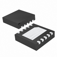
MAX15024AATB+T Maxim Integrated Products, MAX15024AATB+T Datasheet - Page 9

MAX15024AATB+T
Manufacturer Part Number
MAX15024AATB+T
Description
IC GATE DRVR 1CH 16NS 10TDFN-EP
Manufacturer
Maxim Integrated Products
Type
High Speedr
Datasheet
1.MAX15024AATBVT.pdf
(16 pages)
Specifications of MAX15024AATB+T
Configuration
High-Side
Input Type
Inverting and Non-Inverting
Delay Time
16ns
Current - Peak
4A
Number Of Configurations
1
Number Of Outputs
1
Voltage - Supply
4.5 V ~ 28 V
Operating Temperature
-40°C ~ 125°C
Mounting Type
Surface Mount
Package / Case
10-TDFN Exposed Pad
Rise Time
24 ns
Fall Time
16 ns
Supply Voltage (min)
4.5 V
Supply Current
1.5 mA
Maximum Power Dissipation
1481.5 mW
Maximum Operating Temperature
+ 125 C
Mounting Style
SMD/SMT
Maximum Turn-off Delay Time
18 ns
Maximum Turn-on Delay Time
18 ns
Minimum Operating Temperature
- 40 C
Number Of Drivers
1
Lead Free Status / RoHS Status
Lead free / RoHS Compliant
High Side Voltage - Max (bootstrap)
-
Lead Free Status / Rohs Status
Lead free / RoHS Compliant
MAX15024
10
—
—
—
—
—
—
1
2
3
4
5
6
7
8
9
MAX15025A
MAX15025B
PIN
—
—
—
—
—
10
—
_______________________________________________________________________________________
1
2
3
4
5
6
7
8
9
MAX15025C
MAX15025D
Single/Dual, 16ns, High Sink/Source
10
—
—
—
—
—
—
1
2
3
4
5
6
7
8
9
FB/SET
N_OUT
P_OUT
NAME
PGND
OUT2
OUT1
GND
DRV
REG
V
IN+
IN1
IN2
IN2
IN-
EP
CC
LDO Regulator Output Set. Feedback for V
Connect FB/SET to GND for a fixed 10V output REG. Connect FB/SET to a
resistor ladder to set V
Power-Supply Input. Bypass to GND with a low-ESR ceramic capacitor of
1µF. Input of the internal housekeeping regulator and of the main REG
regulator.
Signal Ground
Driver Noninverting Logic Input. Connect to V
Driver 1 Noninverting Logic Input
Driver Inverting Logic Input. Connect to GND when not used.
Driver 2 Noninverting Logic Input
Driver 2 Inverting Logic Input
Power Ground. Sink current return. Source of the internal pulldown
n-channel transistor.
Sink Output. Open-drain n-channel output. N_OUT sinks current for power
MOSFET turn-off.
Driver 2 Output
Source Output. Pullup p-channel output (open drain). Sources current for
power MOSFET turn-on.
Driver 1 Output
Output Driver Supply Voltage. Decouple DRV with a low ESR > 0.1µF
ceramic capacitor to PGND placed in close proximity to the device. DRV
can be powered independently from REG. Connect DRV, REG, and V
together when there is no need for special DRV supply sequencing and
the power-MOSFET gate voltage does not need to be regulated or limited.
Voltage Regulator Output. Connect to DRV for driving the power MOSFET
with regulated V
ceramic capacitor to GND placed in close proximity to the device to
ensure regulator stability.
Exposed Pad. Internally connected to GND. Connect to GND plane or
thermal pad and use multiple vias to a solid copper area on the bottom of
the PCB.
GS
Current Gate Drivers
amplitude. Bypass with a low-ESR 1µF (minimum)
REG
.
FUNCTION
REG
CC
adjustment (V
Pin Description
when not used.
FB
> 200mV).
CC
9


