TC429MJA Microchip Technology, TC429MJA Datasheet - Page 10
TC429MJA
Manufacturer Part Number
TC429MJA
Description
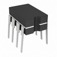
IC MOSFET DRIVER 6A HS 8CDIP
Manufacturer
Microchip Technology
Type
Microcontrollerr
Datasheet
1.TC429CPA.pdf
(18 pages)
Specifications of TC429MJA
Configuration
Low-Side
Input Type
Inverting
Delay Time
53ns
Current - Peak
6A
Number Of Configurations
1
Number Of Outputs
1
Voltage - Supply
7 V ~ 18 V
Operating Temperature
-55°C ~ 125°C
Mounting Type
Through Hole
Package / Case
8-CDIP (0.300", 7.62mm)
Rise Time
35 ns
Fall Time
35 ns
Supply Voltage (min)
7 V
Supply Current
12 mA
Maximum Power Dissipation
800 mW
Maximum Operating Temperature
+ 125 C
Mounting Style
Through Hole
Minimum Operating Temperature
- 55 C
Number Of Drivers
1
Lead Free Status / RoHS Status
Lead free / RoHS Compliant
High Side Voltage - Max (bootstrap)
-
Lead Free Status / Rohs Status
Lead free / RoHS Compliant
Available stocks
Company
Part Number
Manufacturer
Quantity
Price


TC429
The device capacitive load dissipation is:
EQUATION
Quiescent power dissipation depends on input signal
duty cycle. A logic low input results in a low-power
dissipation mode with only 0.5 mA total current drain.
Logic-high signals raise the current to 5 mA maximum.
The quiescent power dissipation is:
EQUATION
Transition power dissipation arises because the output
stage N- and P-channel MOS transistors are ON
simultaneously for a very short period when the output
changes.
The device transition power dissipation is approxi-
mately:
EQUATION
An example shows the relative magnitude for each
item.
DS21416C-page 10
Maximum ambient operating temperature:
Where:
V
P
T
C
D
JA
f
Where:
S
D
J
Where:
f = Switching frequency
C = Capacitive load
V
= 2500 pF
= 15V
= 50%
= 200 kHz
= Package power dissipation:
= P
= 113 mW + 10 mW + 41 mW
= 164 mW
= T
= 150ºC - (150ºC/W)(0.164W)
= 125 C
= Maximum allowable junction temperature
(+150 C)
= Junction-to-ambient thermal resistance
(150 C/W, CERDIP)
S
I
I
D = Duty cycle
H
L
= Supply voltage
P Q
P
= Quiescent current with input low
J
= Quiescent current with input high
C
T
–
+ P
(0.5 mA max)
(5 mA max)
=
=
JA
T
fV
V S D I H
P C
+ P
(P
S
D
3.3
=
Q
)
fCV S
10
+
2
–
9
1 D
A Sec
–
I L
TABLE 4-1:
FIGURE 4-5:
Capability.
4.5
Power-on oscillations are due to trace size, layout and
component placement. A ‘quick fix’ for most applica-
tions that exhibit power-on oscillation problems is to
place approximately 10 k
the MOSFET driver.
Conditions:
1.
2.
3.
Note:
Note:
(5 AMP/DIV)
CERDIP Package (
T
C
500mV/DIV
5V/DIV
A
L
5V
= +25 C
= 2500 pF
POWER-ON OSCILLATION
18V
15V
10V
Ambient operating temperature should not
exceed +85ºC for EPA or EOA devices or
+125ºC for MJA devices.
It is extremely important that all MOSFET
driver applications be evaluated for the
possibility of having high-power oscillations
occur during the power-on cycle.
V
5V
S
OUTPUT
500mV
INPUT
MAXIMUM OPERATING
FREQUENCIES
TIME (5 s/DIV)
Peak Output Current
JA
2003 Microchip Technology Inc.
in series with the input of
=150 C/W)
500 kHz
700 kHz
1.3 MHz
>2 MHz
f
MAX
V
R
S
L
5 s
= 18V
= 0.1
Related parts for TC429MJA
Image
Part Number
Description
Manufacturer
Datasheet
Request
R

Part Number:
Description:
CMOS Power MOSFET Driver
Manufacturer:
Microchip Technology
Datasheet:

Part Number:
Description:
Manufacturer:
Microchip Technology Inc.
Datasheet:
Part Number:
Description:
Manufacturer:
Microchip Technology Inc.
Datasheet:
Part Number:
Description:
Manufacturer:
Microchip Technology Inc.
Datasheet:
Part Number:
Description:
Manufacturer:
Microchip Technology Inc.
Datasheet:
Part Number:
Description:
Manufacturer:
Microchip Technology Inc.
Datasheet:
Part Number:
Description:
Manufacturer:
Microchip Technology Inc.
Datasheet:
Part Number:
Description:
Manufacturer:
Microchip Technology Inc.
Datasheet:
Part Number:
Description:
Manufacturer:
Microchip Technology Inc.
Datasheet: