TC429MJA Microchip Technology, TC429MJA Datasheet - Page 3
TC429MJA
Manufacturer Part Number
TC429MJA
Description
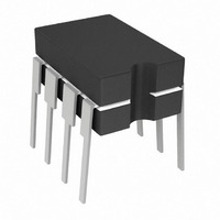
IC MOSFET DRIVER 6A HS 8CDIP
Manufacturer
Microchip Technology
Type
Microcontrollerr
Datasheet
1.TC429CPA.pdf
(18 pages)
Specifications of TC429MJA
Configuration
Low-Side
Input Type
Inverting
Delay Time
53ns
Current - Peak
6A
Number Of Configurations
1
Number Of Outputs
1
Voltage - Supply
7 V ~ 18 V
Operating Temperature
-55°C ~ 125°C
Mounting Type
Through Hole
Package / Case
8-CDIP (0.300", 7.62mm)
Rise Time
35 ns
Fall Time
35 ns
Supply Voltage (min)
7 V
Supply Current
12 mA
Maximum Power Dissipation
800 mW
Maximum Operating Temperature
+ 125 C
Mounting Style
Through Hole
Minimum Operating Temperature
- 55 C
Number Of Drivers
1
Lead Free Status / RoHS Status
Lead free / RoHS Compliant
High Side Voltage - Max (bootstrap)
-
Lead Free Status / Rohs Status
Lead free / RoHS Compliant
Available stocks
Company
Part Number
Manufacturer
Quantity
Price


1.0
Absolute Maximum Ratings †
Supply Voltage ..................................................... +20V
Input Voltage, Any Terminal
Power Dissipation (T
Storage Temperature Range.............. -65°C to +150°C
Maximum Junction Temperature, T
† Stresses above those listed under "Absolute Maximum
Ratings" may cause permanent damage to the device. These
are stress ratings only and functional operation of the device
at these or any other conditions above those indicated in the
operation sections of the specifications is not implied.
Exposure to Absolute Maximum Rating conditions for
extended periods may affect device reliability.
DC ELECTRICAL CHARACTERISTICS
Electrical Specifications: Unless otherwise noted, T
Input
Logic ‘1’, High Input Voltage
Logic ‘0’, Low Input Voltage
Input Current
Output
High Output Voltage
Low Output Voltage
Output Resistance
Peak Output Current
Latch-Up Protection
Withstand Reverse Current
Switching Time (Note 1)
Rise Time
Fall Time
Delay Time
Delay Time
Power Supply
Power Supply Current
Note 1: Switching times ensured by design.
2003 Microchip Technology Inc.
PDIP ............................................................ 730 mW
CERDIP ....................................................... 800 mW
SOIC............................................................ 470 mW
................................... V
ELECTRICAL
CHARACTERISTICS
Parameters
A
70°C)
DD
+ 0.3V to GND – 0.3V
Sym
J
V
I
V
V
V
R
I
REV
t
t
I
PK
t
t
D1
D2
I
IN
OH
OL
R
F
S
............... +150°C
IH
IL
O
V
DD
Min
-10
2.4
– 0.025
—
—
—
—
—
—
—
—
—
—
—
—
A
= +25°C with 7V
Typ
1.8
1.3
1.8
1.5
6.0
0.5
3.5
0.3
23
25
53
60
—
—
—
PIN FUNCTION TABLE
0.025
OUTPUT
OUTPUT
Max
Symbol
0.8
2.5
2.5
5.0
0.5
10
35
35
75
75
—
—
—
—
INPUT
GND
GND
V
V
NC
DD
DD
Units
nsec C
nsec C
nsec Figure 4-1
nsec Figure 4-1
V
mA
µA
DD
V
V
V
V
A
A
Supply input, 7V to 18V
Control input. TTL/CMOS compatible
logic input
No connection
Ground
Ground
CMOS push-pull, common to pin 7
CMOS push-pull, common to pin 6
Supply input, 7V to 18V
18V.
0V
V
V
V
V
V
Duty cycle
V
V
V
IN
OUT
IN
OUT
DD
DD
L
L
IN
IN
= 2500 pF, Figure 4-1
= 2500 pF, Figure 4-1
= 0.8V,
= 2.4V,
= 3V
= 0V
= 18V, Figure 4-4
= 16V
V
= 10 mA, V
= 10 mA, V
IN
Description
V
Conditions
DD
2%, t
DD
DD
DS21416C-page 3
TC429
= 18V
= 18V
300 µsec,
Related parts for TC429MJA
Image
Part Number
Description
Manufacturer
Datasheet
Request
R

Part Number:
Description:
CMOS Power MOSFET Driver
Manufacturer:
Microchip Technology
Datasheet:

Part Number:
Description:
Manufacturer:
Microchip Technology Inc.
Datasheet:
Part Number:
Description:
Manufacturer:
Microchip Technology Inc.
Datasheet:
Part Number:
Description:
Manufacturer:
Microchip Technology Inc.
Datasheet:
Part Number:
Description:
Manufacturer:
Microchip Technology Inc.
Datasheet:
Part Number:
Description:
Manufacturer:
Microchip Technology Inc.
Datasheet:
Part Number:
Description:
Manufacturer:
Microchip Technology Inc.
Datasheet:
Part Number:
Description:
Manufacturer:
Microchip Technology Inc.
Datasheet:
Part Number:
Description:
Manufacturer:
Microchip Technology Inc.
Datasheet: