MCZ33927EK Freescale Semiconductor, MCZ33927EK Datasheet - Page 12
MCZ33927EK
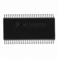
Manufacturer Part Number
MCZ33927EK
Description
IC FET PRE-DRIVER 3PH 54-SOIC
Manufacturer
Freescale Semiconductor
Specifications of MCZ33927EK
Configuration
3 Phase Bridge
Input Type
Inverting and Non-Inverting
Delay Time
265ns
Current - Peak
600mA
Number Of Configurations
1
Number Of Outputs
3
High Side Voltage - Max (bootstrap)
75V
Voltage - Supply
8 V ~ 40 V
Operating Temperature
-40°C ~ 125°C
Mounting Type
Surface Mount
Package / Case
54-SOIC (7.5mm Width) Exposed Pad, 54-eSOIC, 54-HSOIC
Lead Free Status / RoHS Status
Lead free / RoHS Compliant
Available stocks
Company
Part Number
Manufacturer
Quantity
Price


device in a Single Wire CAN communications bus.
Communications takes place from a single pin over a single
wire using a common ground for a current return path. Two
data rates are available, with the high rate used for factory or
assembly line communications and the lower for actual
control its operation and to process and generate the data for
the bus.
GROUND PINS
their number and locations at each of the four corners serve
also to remove heat from the IC. The biggest benefit of this is
obtained by putting a lot of copper on the PCB in this area
and, if ground is an internal layer, by adding numerous
plated-through connections to it with the largest diameter
holes the layout can use.
TXD DATA
TXD pin. A “1” driven on TXD will result in an undriven
(recessive) state (bus at near zero volts). When the TXD pin
is low, the output goes to a driven state. The voltage and
waveshaping in the driven state is determined by the levels
on the MODE0 and MODE1 Pins (refer to
MODE CONTROL
voltage and the IC Sleep mode operation.
mode versus the logic levels on MODE0 and MODE1.
the IC so that in case the pins are not driven, the device will
enter the Sleep mode. This is usually the situation as the
12
Table 6. Mode Control Logic Levels
33897
FUNCTIONAL DESCRIPTION
INTRODUCTION
The 33897 Series is intended for use as a physical layer
The 33897 Series is intended to be used with an MCU to
The four ground pins are not only for electrical conduction,
The data driven onto the SWCAN bus is inverted from the
The MODE pins control the transmitter filtering and BUS
The MODE0 and MODE1 pins have a weak pull-down in
MODE0
0
0
1
1
Logic Level
MODE1
0
1
0
1
Sleep mode
High voltage wake-up mode
High speed mode
Normal mode
Operation
Table 6
Table
FUNCTIONAL DESCRIPTION
FUNCTIONAL PIN DESCRIPTION
6).
shows the
INTRODUCTION
system communications where the radiated EMI of the higher
rate could be an issue.
high speed, and high voltage wake-up).
MCU comes out of reset, before the driving signals have
been configured as outputs.
RXD DATA
on this pin. This pin is a logic high when the bus is in the
recessive state (near zero volts) and is logic low when the
bus is in either the normal or high voltage dominant state.
external resistor to pull it up. When the device is in sleep
mode, the output will be off unless a high voltage wake-up
level is detected on the bus. If the wake-up level is detected,
the output will be driven by the data on the bus. If the level of
the data returns to normal level, the output will return to off
after a short delay unless a non-sleep mode condition is set
by the MCU.
LOAD SWITCH
ground is detected. If this happens, the switch is opened and
the resistor normally attached to its pin will no longer pass
current to or from the bus.
CNTL OUTPUT
When the output is low, the V
shutdown. This is normally used to shut down the MCU and
all the devices powered by V
This is done to save power. When the part is taken out of the
Sleep mode by the higher than normal bus voltage, this pin is
asserted high and the V
regulated level. This starts the MCU, which controls the mode
of the IC. The MCU must change the mode signals to non-
Sleep mode levels in order to keep this pin from going low.
There is a delay to allow the MCU to fully wake-up and take
control after the high voltage signaling is removed before the
level on this output returns low. After a delay time, even if the
bus is at high voltage, the IC will return to Sleep mode if both
MODE pins are low.
Two pins control the mode of operation (sleep, low speed,
The data received on the bus is translated to logic levels
This is an open-drain type of output that requires an
This switch is ON in all operating modes unless a loss of
This logic level signal is used to control a V
Analog Integrated Circuit Device Data
CC
regulator brings its output up to the
CC
CC
when the IC is in Sleep mode.
regulator is expected to
Freescale Semiconductor
CC
regulator.
Related parts for MCZ33927EK
Image
Part Number
Description
Manufacturer
Datasheet
Request
R

Part Number:
Description:
Manufacturer:
Freescale Semiconductor, Inc
Datasheet:
Part Number:
Description:
Manufacturer:
Freescale Semiconductor, Inc
Datasheet:
Part Number:
Description:
Manufacturer:
Freescale Semiconductor, Inc
Datasheet:
Part Number:
Description:
Manufacturer:
Freescale Semiconductor, Inc
Datasheet:
Part Number:
Description:
Manufacturer:
Freescale Semiconductor, Inc
Datasheet:
Part Number:
Description:
Manufacturer:
Freescale Semiconductor, Inc
Datasheet:
Part Number:
Description:
Manufacturer:
Freescale Semiconductor, Inc
Datasheet:
Part Number:
Description:
Manufacturer:
Freescale Semiconductor, Inc
Datasheet:
Part Number:
Description:
Manufacturer:
Freescale Semiconductor, Inc
Datasheet:
Part Number:
Description:
Manufacturer:
Freescale Semiconductor, Inc
Datasheet:
Part Number:
Description:
Manufacturer:
Freescale Semiconductor, Inc
Datasheet:
Part Number:
Description:
Manufacturer:
Freescale Semiconductor, Inc
Datasheet:
Part Number:
Description:
Manufacturer:
Freescale Semiconductor, Inc
Datasheet:
Part Number:
Description:
Manufacturer:
Freescale Semiconductor, Inc
Datasheet:
Part Number:
Description:
Manufacturer:
Freescale Semiconductor, Inc
Datasheet: