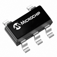
MCP1416T-E/OT Microchip Technology, MCP1416T-E/OT Datasheet - Page 12

MCP1416T-E/OT
Manufacturer Part Number
MCP1416T-E/OT
Description
IC MOSFET DVR 1.5A HS TSOT23-5
Manufacturer
Microchip Technology
Type
Low Sider
Specifications of MCP1416T-E/OT
Number Of Outputs
1
Input Type
Non-Inverting
On-state Resistance
6 Ohm
Current - Peak Output
1.5A
Voltage - Supply
4.5 V ~ 18 V
Operating Temperature
-40°C ~ 125°C
Mounting Type
Surface Mount
Package / Case
SOT-23-5, SC-74A, SOT-25
Rise Time
25 ns
Fall Time
25 ns
Supply Voltage (min)
4.5 V
Supply Current
1.1 mA
Maximum Power Dissipation
390 mW
Maximum Operating Temperature
+ 125 C
Mounting Style
SMD/SMT
Minimum Operating Temperature
- 40 C
Number Of Drivers
1
Lead Free Status / RoHS Status
Lead free / RoHS Compliant
Current - Output / Channel
-
Lead Free Status / Rohs Status
Lead free / RoHS Compliant
Other names
MCP1416T-E/OT
MCP1416T-E/OTTR
MCP1416T-E/OTTR
Available stocks
Company
Part Number
Manufacturer
Quantity
Price
Company:
Part Number:
MCP1416T-E/OT
Manufacturer:
MICROCHIP
Quantity:
12 000
MCP1415/16
4.4
The total internal power dissipation in a MOSFET driver
is the summation of three separate power dissipation
elements.
EQUATION 4-1:
4.4.1
The power dissipation caused by a capacitive load is a
direct function of the frequency, total capacitive load,
and supply voltage. The power lost in the MOSFET
driver for a complete charging and discharging cycle of
a MOSFET is shown in
EQUATION 4-2:
4.4.2
The power dissipation associated with the quiescent
current draw depends upon the state of the input pin.
The MCP1415/16 devices have a quiescent current
draw when the input is high of 0.65 mA (typical) and
0.1 mA (typical) when the input is low. The quiescent
power dissipation is shown in
EQUATION 4-3:
DS22092C-page 12
Where:
Where:
Where:
P
V
V
I
I
P
P
CC
C
DD
QH
DD
P
QL
P
D
Q
T
T
L
f
Q
Power Dissipation
=
CAPACITIVE LOAD DISSIPATION
QUIESCENT POWER DISSIPATION
(
=
=
=
=
=
=
=
=
=
=
=
I
QH
P T
P
L
×
Total power dissipation
Load power dissipation
Quiescent power dissipation
Operating power dissipation
Switching frequency
Total load capacitance
MOSFET driver supply voltage
Quiescent current in the high
state
Duty cycle
Quiescent current in the low
state
=
=
MOSFET driver supply voltage
D
P L
f C
Equation
+
×
I
+
QL
T
P Q
×
Equation
×
V
+
(
DD
1 D
P CC
4-2.
–
2
)
) V
4-3.
×
DD
4.4.3
The operating power dissipation occurs each time the
MOSFET driver output transitions because for a very
short period of time both MOSFETs in the output stage
are on simultaneously. This cross-conduction current
leads to a power dissipation describe in
EQUATION 4-4:
4.5
Proper PCB layout is important in high current, fast
switching circuits to provide proper device operation
and robustness of design. Improper component
placement may cause errant switching, excessive
voltage ringing, or circuit latch-up. PCB trace loop area
and
accomplished by placing the MOSFET driver directly at
the load and placing the bypass capacitor directly at the
MOSFET driver
or ground return traces directly beneath the driver
output signal also reduces trace inductance. A ground
plane will also help as a radiated noise shield as well as
providing some heat sinking for power dissipated within
the device
FIGURE 4-3:
(TOP).
FIGURE 4-4:
(BOTTOM).
Where:
V
CC
inductance
DD
f
PCB Layout Considerations
(Figure
OPERATING POWER DISSIPATION
=
=
=
P CC
(Figure
4-4).
must
Cross-conduction constant
(A*sec)
Switching frequency
MOSFET driver supply voltage
=
Recommended PCB Layout
Recommended PCB Layout
© 2008 Microchip Technology Inc.
CC f
4-3). Locating ground planes
be
×
×
minimized.
V DD
Equation
This
4-4.
is


