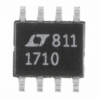
LTC1710CS8 Linear Technology, LTC1710CS8 Datasheet - Page 3

LTC1710CS8
Manufacturer Part Number
LTC1710CS8
Description
IC HISIDE SWTCH SMBUS DUAL 8SOIC
Manufacturer
Linear Technology
Type
High Sider
Datasheet
1.LTC1710CS8.pdf
(8 pages)
Specifications of LTC1710CS8
Input Type
2-Wire SMBus
Number Of Outputs
2
On-state Resistance
400 mOhm
Current - Output / Channel
300mA
Current - Peak Output
1A
Voltage - Supply
2.7 V ~ 5.5 V
Operating Temperature
0°C ~ 70°C
Mounting Type
Surface Mount
Package / Case
8-SOIC (3.9mm Width)
Switch Type
High Side
Power Switch Family
LTC1710
Input Voltage
2.7 to 5.5V
Power Switch On Resistance
550mOhm
Mounting
Surface Mount
Supply Current
17uA
Package Type
SOIC N
Operating Temperature (min)
0C
Operating Temperature (max)
70C
Operating Temperature Classification
Commercial
Pin Count
8
Lead Free Status / RoHS Status
Contains lead / RoHS non-compliant
Available stocks
Company
Part Number
Manufacturer
Quantity
Price
Company:
Part Number:
LTC1710CS8
Manufacturer:
LT
Quantity:
10 000
Part Number:
LTC1710CS8#PBF
Manufacturer:
LINEAR/凌特
Quantity:
20 000
The
temperature range.
Note 1: Absolute Maximum Ratings are those values beyond which the life
of a device may be impaired.
Note 2: Approximately 3% hysteresis is provided to ensure stable operation
and eliminate false triggering by minor V
Note 3: Measured from V
ELECTRICAL CHARACTERISTICS
SYMBOL
t
t
V
V
V
C
I
SMBus Related Specifications (Note 5)
f
t
t
t
t
t
t
t
t
t
t
I
ON
OFF
IN
SMB
BUF
SU:STA
HD:STA
SU:STO
HD: DAT
SU:DAT
LOW
HIGH
f
r
PULL-UP
IL
IH
OL
IN
denotes specifications which apply over the full operating
PARAMETER
Output Turn-On Time
(100 /1 F Load)
Output Turn-Off Time
(100 /1 F Load)
DATA/CLK Input Low Voltage
AD1 Input Low Voltage
DATA/CLK High Voltage
AD1 Input High Voltage
Data Output Low Voltage
Input Capacitance (DATA, CLK, AD1)
Input Leakage Current (DATA, CLK)
Input Leakage Current (AD1)
SMBus Operating Frequency
Bus Free Time Between
Stop and Start
Start Condition Setup Time
Start Condition Hold Time
Stop Condition Setup Time
Data Hold Time
Data Setup Time
Clock Low Period
Clock High Period
Clock/Data Fall Time
Clock/Data Rise Time
Current Through External Pull-Up
Resistor on DATA Pin
CC
> V
UVLO
to SMBus ready for DATA input.
CC
glitches.
CONDITIONS
V
V
V
V
V
V
V
V
V
V
(Open-Drain Data Pull-Down Current Capacity)
CC
CC
CC
CC
CC
CC
CC
CC
CC
CC
= 2.7V (From ON (Note 6) to V
= 5.5V (From ON (Note 6) to V
= 2.7V (From OFF (Note 7) to V
= 5.5V (From OFF (Note 7) to V
= 2.7V to 5.5V
= 2.7V to 5.5V
= 2.7V to 5.5V
= 2.7V to 5.5V
= 2.7V to 5.5V, I
= 2.7V to 5.5V
T
A
= 25 C, V
PULL-UP
Note 4: The oscillator frequency is not tested directly but is inferred from
turn-on time.
Note 5: SMBus timing specifications are guaranteed but not tested.
Note 6: ON is enabled upon receiving the Stop condition from the SMBus
master.
Note 7: OFF is enabled upon receiving the Stop condition from the SMBus
master.
= 350 A
CC
= SW0D = 5V unless otherwise noted.
OUT
OUT
OUT
OUT
= 90% V
= 90% V
= 10% V
= 10% V
CC
CC
CC
CC
)
)
)
)
V
CC
MIN
300
250
100
1.4
4.7
4.7
4.0
4.0
4.7
4.0
10
– 0.2
0.18
TYP
200
160
250
250
5
LTC1710
MAX
1000
100
300
350
0.6
0.2
0.4
50
250
1
UNITS
3
kHz
nA
pF
ns
ns
ns
ns
V
V
V
V
V
A
A
s
s
s
s
s
s
s
s
s
s


