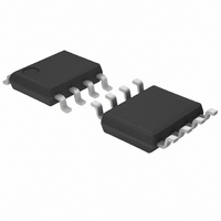
BD2056AFJ-E2 Rohm Semiconductor, BD2056AFJ-E2 Datasheet

BD2056AFJ-E2
Specifications of BD2056AFJ-E2
Related parts for BD2056AFJ-E2
BD2056AFJ-E2 Summary of contents
Page 1
... Dual N-MOS high side switch 2) Continuous current load 0.25A 3) Control input logic Active-Low : BD2046AFJ Active-High : BD2056AFJ 4) Soft start circuit 5) Over current detection 6) Thermal shutdown 7) Under voltage lockout 8) Open drain error flag output ...
Page 2
... Output current at short Output rise time Output turn on time Output fall time T Output turn off time T V UVLO threshold V ○BD2056AFJ (Unless otherwise specified, V Parameter Symbol Operating Current Standby Current /EN input voltage /EN input current /OC output LOW voltage /OC output leak current ON resistance Output current at short ...
Page 3
... BD2046AFJ, BD2056AFJ Measurement circuit V DD 1µF A GND IN OUT1 V EN1 OUT2 EN V EN2 EN Operating current V DD 10k 1µF GND /OC1 IN OUT1 V EN1 OUT2 EN V EN2 /OC2 EN ON resistance, Over current detection Timing diagram ○BD2046AFJ T ON1 90% V OUT 10% T ON2 V 50% EN Fig.2 Timing diagram www.rohm.com © ...
Page 4
... BD2046AFJ, BD2056AFJ Reference data 140 Ta=25°C 120 100 SUPPLY VOLTAGE : V [V] IN Fig.4 Operating current EN,/EN Enable 1.0 V =5.0V IN 0.8 0.6 0.4 0.2 0.0 - 100 AMBIENT TEMPERATURE : Ta[ ℃ ] Fig.7 Operating current EN,/EN Disable 0.5 Ta=25°C 0.4 0.3 0.2 0.1 0.0 ...
Page 5
... BD2046AFJ, BD2056AFJ 5.0 Ta=25°C 4.0 3.0 2.0 1.0 0 SUPPLY VOLTAGE : V [V] IN Fig.16 Output rise time 5.0 V =5.0V IN 4.0 3.0 2.0 1.0 0.0 - 100 AMBIENT TEMPERATURE : Ta[ ℃ ] Fig.19 Output turn on time 6.0 Ta=25°C 5.0 4.0 3.0 2.0 1.0 0 SUPPLY VOLTAGE : V ...
Page 6
... R =20Ω =100uF L TIME (1s/div.) Fig.34 UVLO response Increasing V IN (BD2056AFJ) Regarding the output rise/fall and over current detection characteristics of BD2046AFJ, refer to the characteristic of BD2056AFJ. www.rohm.com © 2009 ROHM Co., Ltd. All rights reserved. V /EN (5V/div.) V /OC (5V/div.) V OUT (5V/div.) V ...
Page 7
... BD2046AFJ, BD2056AFJ Block diagram /EN1 EN1 Gate Logic1 OCD1 IN UVLO /EN2 EN2 OCD2 Gate Logic2 GND Fig.36 Block diagram Pin description ○BD2046AFJ Pin No. Symbol 1 GND / / OUT ○BD2056AFJ Pin No. Symbol 1 GND / OUT www.rohm.com © 2009 ROHM Co., Ltd. All rights reserved. TSD1 /OC1 ...
Page 8
... BD2046AFJ, BD2056AFJ I/O circuit Symbol EN1(/EN1) EN2(/EN2) /OC1 /OC2 OUT1 OUT2 www.rohm.com © 2009 ROHM Co., Ltd. All rights reserved. Pin No /EN1(EN1) /EN2(EN2 /OC1 /OC2 8/13 Technical Note Equivalent circuit OUT1 OUT2 2009.05 - Rev.A ...
Page 9
... BD2046AFJ, BD2056AFJ Functional description 1. Switch operation IN terminal and OUT terminal are connected to the drain and the source of switch MOSFET respectively. And the IN terminal is used also as power source input to internal control circuit. When the switch is turned on from EN/EN control input, IN terminal and OUT terminal are connected by a 100mΩ switch. ...
Page 10
... BD2046AFJ, BD2056AFJ V /EN V OUT I OUT V /OC Fig.38 Over current detection, thermal shutdown timing OUT I OUT V /OC Fig.39 Over current detection, thermal shutdown timing Typical application circuit VBUS IN OUT D+ D- Regulator GND Data www.rohm.com © 2009 ROHM Co., Ltd. All rights reserved. Output shortcircuit ...
Page 11
... BD2046AFJ, BD2056AFJ Application information When excessive current flows owing to output shortcircuit or so, ringing occurs by inductance of power source line to IC, and may cause bad influences upon IC actions. In order to avoid this case, connect a bypath capacitor by IN terminal and GND terminal of IC. 1uF or higher is recommended. ...
Page 12
... BD2046AFJ, BD2056AFJ Notes for use (1) Absolute Maximum Ratings An excess in the absolute maximum ratings, such as supply voltage, temperature range of operating conditions, etc., can break down devices, thus making impossible to identify breaking mode such as a short circuit or an open circuit. If any special mode exceeding the absolute maximum ratings is assumed, consideration should be given to take physical safety measures including the use of fuses, etc ...
Page 13
... BD2046AFJ, BD2056AFJ Ordering part number Part No. Part No. 2046A 2056A SOP-J8 4.9±0.2 (MAX 5.25 include BURR) + 6° 4° −4° 0.545 0.2±0.1 S 1.27 0.42±0.1 0.1 S www.rohm.com © 2009 ROHM Co., Ltd. All rights reserved Package FJ: SOP-J8 <Tape and Reel information> ...
Page 14
No copying or reproduction of this document, in part or in whole, is permitted without the consent of ROHM Co.,Ltd. The content specified herein is subject to change for improvement without notice. The content specified herein is for the purpose ...


