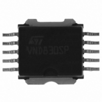
VND830SP13TR STMicroelectronics, VND830SP13TR Datasheet - Page 7

VND830SP13TR
Manufacturer Part Number
VND830SP13TR
Description
IC DRIVER 2CH HI-SIDE POWERSO-10
Manufacturer
STMicroelectronics
Type
High Sider
Datasheet
1.VND830SP13TR.pdf
(27 pages)
Specifications of VND830SP13TR
Input Type
Non-Inverting
Number Of Outputs
2
On-state Resistance
60 mOhm
Current - Peak Output
9A
Voltage - Supply
5.5 V ~ 36 V
Operating Temperature
-40°C ~ 150°C
Mounting Type
Surface Mount
Package / Case
PowerSO-10 Exposed Bottom Pad
Supply Voltage (min)
5.5 V
Supply Current
40 mA
Maximum Power Dissipation
73500 mW
Maximum Operating Temperature
+ 150 C
Mounting Style
SMD/SMT
Minimum Operating Temperature
- 40 C
Switch Type
High Side
Power Switch On Resistance
60mOhm
Output Current
9A
Package Type
PowerSO
Operating Temperature (min)
-40C
Operating Temperature (max)
150C
Operating Temperature Classification
Automotive
Mounting
Surface Mount
Pin Count
10
Lead Free Status / RoHS Status
Contains lead / RoHS non-compliant
Current - Output / Channel
-
Lead Free Status / Rohs Status
Lead free / RoHS Compliant
Other names
497-3306-2
Available stocks
Company
Part Number
Manufacturer
Quantity
Price
Company:
Part Number:
VND830SP13TR
Manufacturer:
PANASONIC
Quantity:
100
Part Number:
VND830SP13TR
Manufacturer:
ST
Quantity:
20 000
VND830SP
2.2
2.3
Note:
Thermal data
Table 4.
1. When mounted on a standard single-sided FR-4 board with 0.5 cm
2. When mounted on a standard single-sided FR-4 board with 6 cm
Electrical characteristics
Values specified in this section are for 8 V < V
otherwise stated.
Figure 3.
V
Fn
Symbol
R
R
to all V
all V
thj-lead
thj-amb
= V
CC
CCn
CC
V
pins. Horizontal mounting and no artificial air flow.
IN1
pins. Horizontal mounting and no artificial air flow.
Thermal resistance junction-lead
Thermal resistance junction-ambient
- V
Thermal data (per island)
Current and voltage conventions
V
STAT1
OUTn
I
IN1
V
IN2
during reverse battery condition.
V
STAT2
I
I
I
STAT2
STAT1
IN2
Parameter
Doc ID 7380 Rev 4
STATUS 2
INPUT 2
STATUS 1
INPUT 1
GND
CC
< 36 V; -40 °C < T
I
OUTPUT 1
OUTPUT 2
GND
2
V
of Cu (at least 35 µm thick) connected to
2
CC
of Cu (at least 35 µm thick) connected
51.7
(1)
Electrical specifications
I
V
j
OUT2
Value
F1
< 150 °C, unless
1.7
V
(*)
OUT2
I
V
OUT1
37
OUT1
(2)
V
I
S
CC
°C/W
°C/W
Unit
7/27


