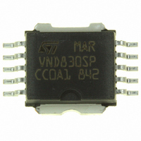
VND830SP STMicroelectronics, VND830SP Datasheet - Page 9

VND830SP
Manufacturer Part Number
VND830SP
Description
IC DRIVER DUAL 36V 6A POWERSO-10
Manufacturer
STMicroelectronics
Type
High Sider
Datasheet
1.VND830SP13TR.pdf
(27 pages)
Specifications of VND830SP
Input Type
Non-Inverting
Number Of Outputs
2
On-state Resistance
60 mOhm
Current - Peak Output
9A
Voltage - Supply
5.5 V ~ 36 V
Operating Temperature
-40°C ~ 150°C
Mounting Type
Surface Mount
Package / Case
PowerSO-10 Exposed Bottom Pad
Supply Voltage (min)
5.5 V
Supply Current
40 mA
Maximum Power Dissipation
73500 mW
Maximum Operating Temperature
+ 150 C
Mounting Style
SMD/SMT
Minimum Operating Temperature
- 40 C
Lead Free Status / RoHS Status
Lead free / RoHS Compliant
Current - Output / Channel
-
Lead Free Status / Rohs Status
Lead free / RoHS Compliant
Other names
497-2709-5
Available stocks
Company
Part Number
Manufacturer
Quantity
Price
Company:
Part Number:
VND830SP
Manufacturer:
TI
Quantity:
6 220
Part Number:
VND830SP
Manufacturer:
ST
Quantity:
20 000
Company:
Part Number:
VND830SP-E
Manufacturer:
IR
Quantity:
3 351
Company:
Part Number:
VND830SP13TR
Manufacturer:
PANASONIC
Quantity:
100
Part Number:
VND830SP13TR
Manufacturer:
ST
Quantity:
20 000
Company:
Part Number:
VND830SPTR-E
Manufacturer:
ST
Quantity:
3 000
VND830SP
Table 8.
Table 9.
Table 10.
Table 11.
dV
dV
Symbol
Symbol
t
t
Symbol
DOL(on)
DOL(off)
V
V
I
C
Symbol
V
LSTAT
V
OUT
OUT
V
I
I(hyst)
V
STAT
V
STAT
I
SCL
OL
t
t
I
OL
d(on)
d(off)
IH
ICL
IL
IH
IL
/dt
/dt
(on)
(off)
Open-load on-state detection threshold
Open-load on-state detection delay
Open-load off-state voltage detection
threshold
Open-load detection delay at turn-off
Status low output voltage
Status leakage current
Status pin Input capacitance
Status clamp voltage
Input low level
Low level input current
Input high level
High level input current
Input hysteresis voltage
Input clamp voltage
Switching (V
Logic inputs
Status pin
Open-load detection
Turn-on delay time
Turn-off delay time
Turn-on voltage slope
Turn-off voltage slope
Parameter
Parameter
Parameter
Parameter
CC
= 13V; T
Doc ID 7380 Rev 4
R
edge to V
(see
R
edge to V
(see
R
to V
(see
R
to V
L
L
L
L
= 6.5
= 6.5
= 6.5
= 6.5
j
OUT
OUT
V
V
I
I
I
Normal operation;
V
Normal operation;
V
I
I
IN
IN
STAT
STAT
STAT
Figure
Figure
Figure
= 25°C)
IN
IN
STAT
STAT
= 1 mA
= -1 mA
Test conditions
= 1.25 V
= 3.25 V
= 10.4 V
= 1.3 V (see
Test conditions
= 1.6 mA
= 1 mA
= - 1 mA
OUT
OUT
Test conditions
= 5 V
= 5 V
from V
from V
from V
from V
5)
5)
5)
= 1.3 V
= 11.7 V
V
I
OUT
V
Test conditions
IN
IN
OUT
OUT
IN
IN
= 5 V
= 0 V
= 0 A
rising
falling
Figure
= 11.7 V
= 1.3 V
5)
Min.
3.25
Min.
0.5
—
—
—
—
1
6
Electrical specifications
Min.
Min.
1.5
6
50
Figure 19
Figure 21
Typ.
-0.7
6.8
Typ.
See
See
30
30
Typ.
-0.7
Typ. Max.
6.8
100
2.5
Max.
1.25
Max.
1000
10
100
200
200
8
0.5
3.5
Max. Unit
10
8
—
—
—
—
Unit
Unit
Unit
V/µs
V/µs
mA
µA
µA
µA
pF
µs
µs
V
V
V
V
V
V
µs
µs
V
V
V
9/27


