NUD3105DMT1G ON Semiconductor, NUD3105DMT1G Datasheet
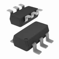
MOSFET N-CH DUAL 6V 500MA SC74-6

NUD3105DMT1G

Manufacturer Part Number
NUD3105DMT1G
Description
MOSFET N-CH DUAL 6V 500MA SC74-6
Manufacturer
ON Semiconductor
Type
Low Sider
Datasheet

Specifications of NUD3105DMT1G

Input Type
Non-Inverting
Number Of Outputs
2
On-state Resistance
1.2 Ohm
Current - Output / Channel
400mA
Current - Peak Output
500mA
Operating Temperature
-40°C ~ 85°C
Mounting Type
Surface Mount
Package / Case
SC-74-6
Configuration
Dual
Transistor Polarity
N-Channel
Resistance Drain-source Rds (on)
0.9 Ohm @ 5 V
Drain-source Breakdown Voltage
6 V
Gate-source Breakdown Voltage
6 V
Continuous Drain Current
0.5 A
Power Dissipation
380 mW
Maximum Operating Temperature
+ 85 C
Mounting Style
SMD/SMT
Minimum Operating Temperature
- 40 C
Supply Voltage Max
6V
No. Of Outputs
2
Output Voltage
6V
Output Current
400mA
Driver Case Style
SC-74
Device Type
Relay
Termination Type
SMD
No. Of Pins
6
Rohs Compliant
Yes
Supply Voltage Min
3V
Peak Reflow Compatible (260 C)
Yes
Leaded Process Compatible
Yes
Filter Terminals
SMD
Lead Free Status / RoHS Status
Lead free / RoHS Compliant
Voltage - Supply
-
Lead Free Status / Rohs Status
Lead free / RoHS Compliant
Other names
NUD3105DMT1GOS
NUD3105DMT1GOS
NUD3105DMT1GOSTR

Available stocks

Company
Part Number
Manufacturer
Quantity
Price
Part Number:
NUD3105DMT1G
Manufacturer:
ON
Quantity:
1 305
Part Number:
NUD3105DMT1G
Manufacturer:
ON/安森美
Quantity:
20 000
NUD3105D
Integrated Relay,
Inductive Load Driver
solenoids incandescent lamps, and small DC motors without the need
of a free−wheeling diode. The device integrates all necessary items
such as the MOSFET switch, ESD protection, and Zener clamps. It
accepts logic level inputs thus allowing it to be driven by a large
variety of devices including logic gates, inverters, and
microcontrollers.
Features
Typical Applications
© Semiconductor Components Industries, LLC, 2009
October, 2009 − Rev. 5
Gate (2)
This device is used to switch inductive loads such as relays,
Sensitive Logic Circuits
Systems Operation
Cassette Recorders
Equipment, Garage Door Openers
Lamp Drivers
Provides a Robust Driver Interface Between D.C. Relay Coil and
Optimized to Switch Relays from 3.0 V to 5.0 V Rail
Capable of Driving Relay Coils Rated up to 2.5 W at 5.0 V
Internal Zener Eliminates the Need of Free−Wheeling Diode
Internal Zener Clamp Routes Induced Current to Ground for Quieter
Low V
Pb−Free Package is Available
Telecom: Line Cards, Modems, Answering Machines, FAX
Computers and Office: Photocopiers, Printers, Desktop Computers
Consumer: TVs and VCRs, Stereo Receivers, CD Players,
Industrial: Small Appliances, Security Systems, Automated Test
Automotive: 5.0 V Driven Relays, Motor Controls, Power Latches,
DS(on)
Reduces System Current Drain
300 k
1.0 k
INTERNAL CIRCUIT DIAGRAMS
Source (1)
Drain (6)
CASE 318F
Source (4)
Drain (3)
1.0 k
300 k
1
Gate (5)
†For information on tape and reel specifications,
NUD3105DMT1
NUD3105DMT1G
including part orientation and tape sizes, please
refer to our Tape and Reel Packaging Specification
Brochure, BRD8011/D.
Relay, Inductive Load Driver
CASE 318F
6
STYLE 7
Device
(Note: Microdot may be in either location)
SC−74
0.5 Amp, 8.0 V Clamp
ORDERING INFORMATION
1
JW4
D
G
http://onsemi.com
= Specific Device Code
= Date Code
= Pb−Free Package
Package
(Pb−Free)
SC−74
SC−74
Publication Order Number:
MARKING
DIAGRAM
3000/Tape & Reel
3000/Tape & Reel
JW4 D G
Shipping
G
NUD3105D/D

Related parts for NUD3105DMT1G

NUD3105DMT1G Summary of contents

Page 1

... Semiconductor Components Industries, LLC, 2009 October, 2009 − Rev. 5 Relay, Inductive Load Driver CASE 318F NUD3105DMT1 NUD3105DMT1G †For information on tape and reel specifications, including part orientation and tape sizes, please refer to our Tape and Reel Packaging Specification Brochure, BRD8011/D. Drain (3) Gate (5) 1 ...

Page 2

MAXIMUM RATINGS (T = 25°C unless otherwise specified) J Symbol V Drain to Source Voltage − Continuous DSS V Gate to Source Voltage – Continuous GS I Drain Current – Continuous D E Single Pulse Drain−to−Source Avalanche Energy ( z ...

Page 3

TYPICAL ELECTRICAL CHARACTERISTICS (T Symbol DYNAMIC CHARACTERISTICS C Input Capacitance iss (V = 5.0 V kHz Output Capacitance oss ( kHz) ...

Page 4

T = 25° 5 1.0 V 0.1 V 0.01 0.001 0.0001 V 0.00001 0 0.1 0.2 0.3 0 DRAIN TO SOURCE VOLTAGE (V) DS Figure 2. Output Characteristics 1200 I = 0.5 ...

Page 5

I , DRAIN CURRENT (A) D Figure 8. On−Resistance vs. Drain Current and Temperature 1 3 ...

Page 6

Designing with this Data Sheet 1. Determine the maximum inductive load current (at max V , min coil resistance & usually minimum CC temperature) that the NUD3105D will have to drive and make sure it is less than the max ...

Page 7

Max Continuous Current Calculation for TX2−5V Relay 178 W Nominal @ R Assuming ±10% Make Tolerance 178 W * 0.9 = 160 W Min @ T = 25° for Annealed Copper Wire is 0.4%/°C ...

Page 8

... Pb−Free strategy and soldering details, please download the ON Semiconductor Soldering and Mounting Techniques Reference Manual, SOLDERRM/D. ON Semiconductor and are registered trademarks of Semiconductor Components Industries, LLC (SCILLC). SCILLC reserves the right to make changes without further notice to any products herein ...

Related keywords